The current progress of localization in the semiconductor industry chain is a topic of interest. Today, we will discuss the situation starting from photoresist, which is a key product in the photolithography process. The “small matter” in the title refers to the twists and turns in the progress of the photoresist project.Localization in semiconductors is a systematic project involving a large number of different production equipment and materials. While photolithography machines are undoubtedly our primary focus, it is not enough to localize just the photolithography machines. Today, we will look at the progress and challenges of semiconductor localization from the announcement of a domestic semiconductor production materials company.Photoresist is an essential product for the critical photolithography process in chip manufacturing. A domestic company responsible for the research and production of photoresist undertook the national “02 Special” project for the “Development and Industrialization of ArF Photoresist” in 2018.In November 2020, the company announced a plan to issue stocks to specific investors (not general shareholders), with a total fundraising amount not exceeding 635 million yuan (including principal). The net amount after deducting issuance costs will be used for the photoresist project, the expansion of a 2000 tons/year nitrogen trifluoride production facility, and to supplement working capital.
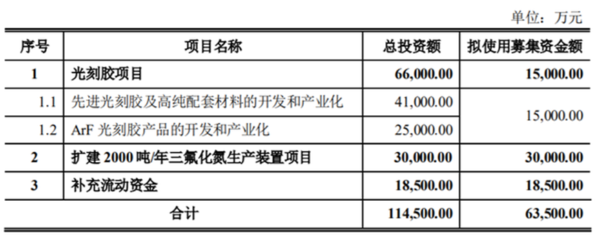
This project includes two main components for photoresist: one is the development and industrialization of advanced photoresist and high-purity supporting materials. The construction involves establishing a large-scale production line for high-purity developer solutions, including synthesis, purification, analysis, and filling processes, as well as analytical and testing equipment. Additionally, the first advanced photoresist analysis and testing center in the country will be established, including immersion lithography machines, coating and developing integrated machines, and key measurement equipment such as CD-SEM.Once the project reaches full production, it will establish a photoresist R&D center, an advanced photoresist analysis and testing center, and a production line with an annual output of 350 tons of high-purity developer solutions.The second component is the development and industrialization of ArF photoresist products: establishing an ArF photoresist production line that includes high-grade ultra-clean rooms, capable of producing ArF photoresist products; establishing production capabilities for key component materials supporting ArF photoresist, and improving the supply of raw materials for photoresist.Once the project reaches full production, it will establish a production line with an annual output of 5 tons of ArF dry photoresist, a production line with an annual output of 20 tons of ArF immersion photoresist, and a production line with an annual output of 45 tons of high-purity reagents supporting photoresist.On March 31, 2021, the company responded to an inquiry regarding the stock issuance to specific investors, clarifying that the main difference between this fundraising project and the “02 Special” project is: on one hand, in terms of product scope, this fundraising project will carry out research and development of photoresist raw materials and promote the R&D and industrialization of supporting materials and developer solutions, aiming to achieve independent research and production of upstream materials for ArF photoresist, further ensuring the self-controllability of the entire industrial chain for domestic ArF photoresist, which is an extension and continuation of the construction goals of the “02 Special” project.On the other hand, the main content of the fundraising project continues to deepen based on the goals proposed in the “02 Special” project, such as the “photoresist testing and evaluation platform” will introduce more advanced testing and evaluation equipment based on the goal of establishing the first ArF photoresist product lithography evaluation testing center in the country under the “02 Special” project, enhancing the evaluation testing capabilities of the center.Based on the previous R&D achievements of the “02 Special” project, the company will further enrich the product types, improve technical indicators, and revise the evaluation system.In the announcement on March 31, 2021, the company also stated: “The construction of the ArF photoresist production line is progressing steadily, and small batches of photoresist products have been produced for customer verification. The cleanroom required for the photoresist project has been basically completed, and the main advanced lithography equipment required for this fundraising project, such as ASML immersion lithography machines, CD-SEM (scanning electron microscope for feature size measurement), and coating and developing integrated machines, have been installed and put into use. The resolution of the above equipment meets the requirements for the 7nm node, and the basic conditions for the development and mass production of ArF photoresist and supporting materials have been established.The company is orderly purchasing the remaining auxiliary equipment to accelerate the smooth implementation of the project.In December 2020, the self-developed ArF photoresist product successfully passed the usage certification from Wuhan Xinxin Integrated Circuit Manufacturing Co., Ltd. (a subsidiary of Yangtze Memory), becoming the first domestically produced ArF photoresist to pass product verification, marking a key breakthrough in industrialization.This verification used a 50nm flash memory technology platform, and in terms of feature size, the line process can meet the photolithography requirements of 45nm-90nm, while the hole process can meet the photolithography requirements of 65nm-90nm. The photoresist product verified on this process platform is representative and technologically advanced in the industry, laying a solid foundation for achieving the project’s ultimate goals. Currently, the issuer’s photoresist products are continuing to be sent to multiple downstream customers for verification work.It is worth noting that the announcement made by the company in March 2021 was quite positive, as the photoresist used in the 50nm flash memory technology platform has passed verification, and several other customers are also in the verification process, awaiting project completion and mass production by the end of 2021.However, a year later, on March 31, 2022, the company announced a one-year delay for the ArF photoresist project: “According to the current actual construction progress of the fundraising investment project, the planned completion deadline for this project has been extended from the original plan of December 31, 2021, to December 31, 2022. The company will continue to coordinate efforts to promote the project construction as soon as possible.”On July 4, 2022, the company issued another announcement disclosing the risk of “the fundraising project being unable to be implemented according to the planned progress,” stating that “the current product verification progress still has uncertainties, and it cannot be ruled out that the previous fundraising photoresist project may not be implemented according to the planned progress.” This means that completing the project by the end of 2022 also carries risks. So, what are the challenges of localization?In the announcement from July 2022, it was mentioned:1: The high-end photoresist field, represented by ArF photoresist, has long been dominated by foreign giants such as Japan Synthetic Rubber, Tokyo Ohka, Shin-Etsu Chemical, and Fujifilm Electronic Materials. Currently, the supply of imported raw materials is affected by international trade, and the verification needs and standards of downstream integrated circuit customers have changed.Moreover, since photoresist (especially 193nm ArF and EUV photoresist for high-process chips) is a highly refined chemical with significant challenges in R&D and industrialization, it has diverse and high requirements in terms of resolution (critical dimension size), contrast (the steepness of the transition from exposed to non-exposed areas), sensitivity (minimum exposure amount), viscosity (thickness of the colloid), adhesion (strength of adhesion to the substrate), etch resistance (ability to maintain adhesion), surface tension, storage, and transportation. Non-compliance with photoresist specifications or unstable quality can lead to a significant decrease in chip product yield, so wafer fabs are generally cautious about large-scale replacement of photoresist.Additionally, the COVID-19 pandemic has significantly impacted the previous fundraising photoresist project, specifically in terms of delays in improvement and debugging work to meet changes in downstream demand, reduced verification efficiency, difficulties in outsourcing testing, and increased challenges in equipment maintenance and repair. If domestic outbreaks continue to occur on a large scale, leading to frequent restrictions on personnel movement and logistics due to epidemic prevention policies, it will adversely affect the implementation of the previous fundraising photoresist project.2: The proposed industrialization of 193nm ArF photoresist products still requires a long time for customer verification to reach a relatively mature state for mass production. Furthermore, due to the variability and complexity of downstream demand, the types of products currently being sent for verification by the issuer cannot fully cover the different process and application needs of various downstream customers.Therefore, even if the issuer’s current focus on the industrialization of ArF photoresist sub-products progresses smoothly, it still faces market competition pressure from imported enterprises and other domestic suppliers.Currently, more mature domestic wafer fabs mostly adopt a “substitution verification” approach when verifying domestic photoresist, requiring that domestic products fully match the performance of the photoresist currently used by the fabs, with high-end process error requirements within a range of +/- 2nm to meet their existing production line and process requirements, thereby reducing their debugging costs.At the same time, due to different chip processes and applications, even if they are both 193nm ArF photoresist, different customers’ production lines and processes will have significantly different parameter requirements, leading to variations in the formulations of corresponding photoresist products.For example, LANs base line layers have different requirements for photoresist due to variations in line width, wiring scale, and line spacing; hole column photoresist has specific requirements for parameters due to different hole sizes; and metal wiring layers require multiple iterations of the entire production process from image to product, with different parameter requirements for each iteration.Moreover, different chip types, such as memory chips and logic chips, have different verification requirements for photoresist.Thus, the company’s ArF photoresist products not only need to conduct product verification for different customer needs but also, due to the aforementioned different usage requirements arising from different processes and stages, even for the same customer, multiple products need to be sent for verification simultaneously, and each must be verified individually. Only after passing comprehensive verification of multiple product groups can they be adopted.Therefore, although the company currently has a certain first-mover advantage in the field of 193nm ArF photoresist, there is still a risk of diminishing relative advantages compared to other domestic suppliers in the high-end photoresist field.Additionally, the high-end photoresist field, represented by ArF photoresist, has long been dominated by foreign giants such as Japan Synthetic Rubber, Tokyo Ohka, Shin-Etsu Chemical, and Fujifilm Electronic Materials. Since photoresist products require long-term trial production and adjustment with downstream customers, and downstream customers have a strong attachment to existing products, new products require a long verification period to ensure compatibility, performance stability, and impurity purity levels that meet or exceed those of existing imported products.If the international trade environment improves in the future, and restrictions on exports to China from major countries are relaxed, the risk of supply disruptions or limited supply of high-end photoresist products may decrease, which could weaken downstream customers’ demand for domestic alternatives, thereby adversely affecting the company’s ArF photoresist product R&D and industrialization process.3. The risk of being unable to guarantee mass production of certain products due to equipment shortages.Defect detection equipment is primarily used for detecting defects in patterns after photolithography and is essential for the preparation of photoresist used in chips with processes of 28nm and below. Factors such as particles and micro bridging can lead to defects in patterns, and as chip processes continue to shorten and volumes decrease, it becomes increasingly difficult to identify particle defects on bare silicon wafers or coated monitoring wafers that can lead to yield loss.Defect detection systems can identify defect issues early, allowing for adjustments and changes to the photoresist product formulation to reduce and eliminate defects.The production lines related to the previous fundraising photoresist project that the company is currently building have been completed, covering multiple models of products used for chips with processes of 28-90nm, and the company will actively adjust formulations based on verification results to produce products that meet customer production needs.However, there is a risk that the import channels for some mass production-required equipment may be blocked, and due to the slowdown in testing progress by domestic equipment suppliers, there may be a lack of available alternative equipment.As the company’s photoresist product R&D and verification work progresses, the lack of key equipment will pose challenges for the industrialization of photoresist used in chips with processes of 28nm and below, thereby affecting the overall implementation progress of the fundraising project.From the above series of announcements, we can see the progress and difficulties of China’s semiconductor localization through the key technology product of photoresist. The “02 Special” ArF photoresist industrialization project, which started in 2018, has faced risks of not being completed even after more than four years, with one of the difficulties being that the original goals of the “02 Special” project have become outdated due to changes in the international environment, leading the company to need to raise funds to localize upstream raw materials and supporting materials for photoresist to achieve self-controllability.Another difficulty is that the user stickiness of photoresist is very high; different production lines, and even the same production line using different processes, will require different photoresists. This means that there is not a single customer sample of one type of photoresist for verification, but rather multiple products need to be verified across different production lines and processes, naturally extending the verification time. Moreover, the products currently sent for verification by the company cannot meet all customer requirements, meaning that the products being sent for verification can only complete the domestic substitution of some types of ArF photoresist.At the same time, domestic wafer fabs mostly adopt a “substitution verification” approach when verifying domestic photoresist, requiring that domestic products fully match the performance of the photoresist currently used by the fabs. The reason for this requirement is that they do not want to incur additional costs for re-tuning production line equipment due to the introduction of new parameter materials.Another difficulty is that with the increase in U.S. sanctions, although the production equipment for the photoresist production line has been purchased, there is still a risk that key defect detection equipment may not arrive, so the company is still verifying products from domestic equipment suppliers.Despite these challenges, I still believe that compared to the past, the domestic semiconductor industry is currently in the best position in history. I think the biggest difficulty in semiconductor localization in the past was establishing a commercial cycle, but this issue has been resolved by the U.S.What is a commercial cycle? It is when every link in the industry chain has sufficient benefits to gain, thus creating a strong drive to engage in activities and a high level of enthusiasm for technological development.Once a commercial cycle is established, it can mobilize everyone’s enthusiasm and create a powerful driving force. During the Cold War between the U.S. and the Soviet Union, the Soviet Union did not solve this problem well. Although it had a population of over 200 million, the self-motivation for production and R&D was not truly mobilized, and its technological progress relied mainly on state-planned military projects and leadership will.In contrast, the U.S. and the West established a good commercial cycle during the same period, where both commercial and technical talents could gain enormous benefits from innovation, R&D, and entrepreneurship within this cycle, thus generating tremendous motivation. A large number of elites in the U.S. could benefit from the commercial cycle, unleashing a great force of innovation, and the development of civilian technology and industry, in turn, provided funding and technology for military development, achieving a good dual drive, which also foreshadowed the end of the Cold War between the U.S. and the Soviet Union.The greatest success of China’s reform and opening up has been the establishment of a commercial cycle, which has mobilized the enthusiasm of the people. In many industries, the government is only responsible for providing taxes, infrastructure, laws, international relations, and public services such as transfer payments, while a large number of private enterprises can earn money through their commercial efforts, resulting in strong motivation. Companies like Huawei, DJI, Xiaomi, and BYD are among the leaders, and many small and medium-sized private enterprises in Zhejiang Province have exported overseas, gaining significant wealth.However, the problem with a purely commercial cycle is that it is based on profit maximization. This means that if purchasing products from foreign companies can yield the greatest commercial benefits, companies will naturally choose to procure from foreign suppliers, leaving domestic suppliers with no opportunities unless they can achieve or exceed the level of their Western counterparts in terms of returns (e.g., lower prices, better services, better technology). Achieving this, especially in the complex technology of the semiconductor industry, requires collaborative innovation with manufacturers across the industry chain, including chip design companies, chip manufacturing companies, and chip production equipment manufacturers, which are mutually beneficial. Whether it is chip design companies or chip production equipment manufacturers, they will send engineers to work on-site for long-term collaboration, indicating that innovation in all aspects of chips is interconnected. If there are no opportunities to gain support from the industry chain and obtain opportunities for product introduction and verification, continuous progress is out of the question, let alone leading the way.Since 2018, U.S. sanctions on chips have significantly changed the profit maximization situation in the commercial cycle. Chinese companies in this cycle can no longer maximize their interests by continuing to purchase U.S. chips, software, and equipment, as there is a risk of being unable to expand production, reduce production, or even shut down. Therefore, they have begun to procure and support domestic chip, equipment, software, and material manufacturers, allowing domestic companies that previously had no opportunities to join the commercial cycle of various industries needing chips in China and gradually grow.Solving the entry problem of the commercial cycle for domestic chips, equipment, software, and materials has essentially resolved the biggest issue. Even if the products you create initially are not perfect or are technically low-end, you can still gain entry into the commercial cycle. The better you do, the greater the benefits you can gain from this commercial cycle, thus achieving gradual domestic substitution.In recent years, the degree of localization in the semiconductor industry chain has been continuously improving, and it is still progressing. This commercial cycle will drive the localization rate to continue to rise.The example of photoresist illustrates this point. The company’s announcement even lists the relaxation of sanctions as a risk item, stating, “If the international trade environment improves in the future, and restrictions on exports to China from major countries are relaxed, the risk of supply disruptions or limited supply of high-end photoresist products may decrease, which could weaken downstream customers’ demand for domestic alternatives, thereby adversely affecting the company’s ArF photoresist product R&D and industrialization process.”In addition to developing photoresist, the company currently generates significant revenue from electronic special gases used in semiconductors (chips, LEDs). In the first nine months of 2022, the company achieved operating revenue of 1.259 billion yuan, a year-on-year increase of 77.64%, and a net profit attributable to shareholders of the listed company of 211 million yuan, a year-on-year increase of 70.33%. Such performance is closely related to the wave of localization.On the other hand, U.S. export controls on production equipment have led the company to verify domestic suppliers of photoresist defect detection equipment. Without the increased U.S. controls, the company might not have given domestic equipment opportunities, as it faces pressure to complete the mass production of the ArF photoresist project. If purchasing U.S. equipment could achieve that, it would certainly prioritize buying advanced and mature products.Moreover, we can also see that China, due to its large scale and capital, has multiple domestic companies developing in the relatively small field of ArF photoresist. Therefore, even though the company believes it is ahead in the progress of ArF photoresist, it also acknowledges in its announcement the risk of “diminishing relative advantages compared to other domestic suppliers.”Additionally, it is worth noting that we should be grateful for the early layout of the “02 Special,” which allowed the company’s ArF photoresist industrialization project to start in 2018. This means that China has been tackling this project for over four years, accumulating considerable experience. This early layout has established seed players for the localization of the semiconductor industry chain and has also won some time. While the continuous expansion of U.S. sanctions has increased the technical difficulties of localization, it has also helped us solve the problem of the commercial cycle, preventing products developed under special projects from entering a state of technical reserve after passing acceptance without being widely applied in the commercial market, which was a very difficult problem to solve in the past.Today’s article reflects my thoughts on the localization of the semiconductor industry chain. We should not underestimate the difficulty of high-tech industrialization; it has a very high technical threshold, requires long-term experience accumulation and learning, and will be obstructed by various factors. If it were easy, it would not be called high-tech or core technology, and it would be easily mastered by countries around the world. Instead, it has a high threshold, as seen in the photoresist project mentioned in this article, which has faced a one-year delay due to various reasons and may continue to be delayed.However, we should not be pessimistic. We do not lack money or markets, and the commercial cycle is profitable. With multiple different companies tackling the challenges, the entire industry is collectively promoting localization, and there will certainly be a resolution in the end. Even if the products created initially have gaps, they can gradually grow within the commercial cycle and generate financial returns.In fact, if we look at various information on the localization of other fields in the semiconductor industry, we can draw the same conclusion.The above are my thoughts on the localization of the semiconductor industry.Previous article links: The Three Huge Potential Development Spaces of China, Psychological Construction for Becoming the World’s First, Coal, Industry, and Food – Looking at the Strategic Position of North China from the Early Days of the Founding of the Country, Thoughts After More Than Seven Months of the Russia-Ukraine War, Why We Maintain Neutrality – Starting from the Cooperation Between China and Ukraine After the Dissolution of the Soviet Union.