In today’s rapidly evolving electronics industry, the customization capabilities of PCB circuit boards have become a core driving force for product innovation and market competition. With over a decade of deep engagement in the PCB manufacturing field, we provide global customers with full lifecycle support from prototype development to mass production, leveraging the integration of technological research and development, flexible production, and comprehensive quality control to help electronic devices achieve performance leaps and rapid market entry.
1. Technology-Driven: High-Precision Processes Meet Complex Design Requirements
Our core competitiveness lies in technological breakthroughs, covering a full range of custom circuit boards from 1 to 14 layers, including single-sided, multi-layer, impedance boards, and blind/buried hole boards, to meet diverse scenario requirements from consumer electronics to industrial control.
-
Extreme Process Parameters: Supports minimum line width and spacing of 3 mil (0.076 mm) and minimum drill hole of 8 mil (0.2 mm). Coupled with HDI (High-Density Interconnect) technology, it enables high-density integration of complex circuits, suitable for high-precision scenarios such as 5G communication modules and medical imaging equipment.
-
Custom Special Materials: Offers a variety of material options including FR-4 (conventional substrate), aluminum substrates (for heat dissipation), ceramic substrates (high-frequency insulation), and Rogers/Arlon high-frequency materials (for RF antennas), meeting special performance requirements for wide temperature ranges from -55℃ to 150℃ and high-frequency transmission above 10GHz.
-
Structural Innovation Support: Supports customized forms such as irregular cutting, metal-based composite structures, and rigid-flex boards, for example, a 0.2mm ultra-thin flexible board developed for wearable devices, or a thick copper (6oz) high-current carrying circuit board designed for new energy vehicles.
-
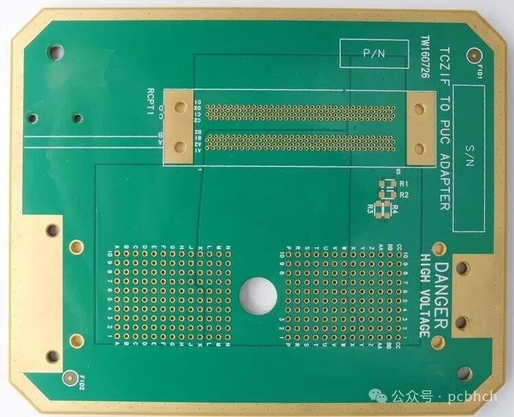
2. Flexible Production: One Piece Minimum Order, Rapid Delivery Shortens R&D Cycle
We understand the importance of R&D efficiency for product market launch. Through intelligent production line layout and lean production management, we have built an industry-leading rapid response capability:
-
Full-Scale Order Coverage: Whether it is a single functional verification sample or a mass production order of 100,000 pieces, we can flexibly accommodate. The “one piece minimum order” model significantly reduces R&D costs for small and medium enterprises, while modular production lines can quickly scale up for bulk orders to meet peak season capacity demands.
-
Industry-Leading Delivery Times: Samples can be delivered in as fast as 24 hours (for double-sided boards), 72 hours for 4-6 layer boards, and production of high multi-layer boards (10 layers and above) completed within 5 days, reducing the average industry cycle by 50%. For example, a medical device client used our expedited service to compress their new product R&D cycle from 3 months to 45 days, successfully seizing market opportunities.
-
Intelligent Production Scheduling System: Utilizes an MES (Manufacturing Execution System) to monitor order progress in real-time, combined with a “parallel processing of previous processes + flexible scheduling of subsequent processes” mechanism, ensuring efficient collaboration between expedited and regular orders, achieving a delivery on-time rate of 99.8%.
-
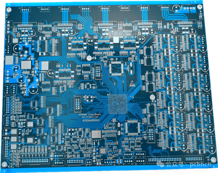
3. Comprehensive Quality Control: International Standards Ensure 99.5%+ Yield Rate
Quality is the lifeline of products. We aim for **”zero defects”** and have established a comprehensive quality control system from raw materials to finished products:
-
Strict Material Selection: Deep collaboration with leading substrate suppliers such as Shengyi and Jialin, all boards are UL certified, with copper foil purity ≥99.98%, ensuring stability in circuit signal transmission and aging resistance.
-
Intelligent Inspection System: Equipped with fully automated AOI optical inspection (precision for 01005 components), X-Ray non-destructive testing (for blind/buried hole quality), flying probe testing (for continuity verification), and 8-zone reflow soldering (99.9% soldering yield), achieving 100% online monitoring during production.
-
International Certification Endorsement: Strictly implementing ISO9001 quality management system, UL safety certification (Document No. E499889), and RoHS 2.0 environmental standards, with product yield rates stable above 99.5% and failure analysis response time ≤24 hours.
4. Scenario-Based Solutions: Addressing Technical Pain Points Across Multiple Fields
We deeply understand the technical characteristics of different industries and provide scenario-based customization services to solve the balance challenges between performance, reliability, and cost for electronic devices:
-
Industrial Control Field: For PLC controllers, servo drives, and other devices, we develop wide-temperature circuit boards (-40℃ to 85℃), using thick copper (3oz) and gold plating processes to enhance corrosion resistance and current carrying efficiency, with an average MTBF (Mean Time Between Failures) exceeding 50,000 hours.
-
Medical Equipment Field: Custom bio-compatible PCBs for monitors and ultrasound devices, certified by ISO13485, with a matte green solder mask design to reduce glare, suitable for the precision operation environment of operating rooms.
-
Automotive Electronics Field: Automotive-grade PCBs meet AEC-Q100 Grade 2 standards, supporting temperature cycling from -40℃ to 105℃, passing 1000 hours of salt spray testing, suitable for safety-critical components such as onboard radar and autonomous driving domain controllers.
-
Consumer Digital Field: Providing ultra-thin (0.4mm), ultra-light (30% lighter than traditional solutions) high-density circuit boards, supporting wireless charging and fast charging protocol integration, helping products like TWS earbuds and smartwatches achieve extreme miniaturization.
5. One-Stop Service: Full-Link Support from Design to Delivery
We break the traditional manufacturing enterprise’s “production-oriented” model, centering on customer needs and providing value-added services covering the entire product lifecycle:
-
Design Optimization: Our professional engineering team is available 24/7, providing DFM (Design for Manufacturability) analysis, such as optimizing pad layouts to reduce soldering defects and adjusting impedance matching to enhance signal integrity, lowering R&D trial and error costs.
-
Vertical Integration Capability: Streamlining the entire chain from “PCB design → prototyping → SMT assembly → finished product testing”, supporting BOM list procurement, PCBA assembly, and functional aging testing, allowing customers to directly obtain “plug-and-play” finished modules, reducing supply chain complexity.
-
Cost Optimization Solutions: By material substitution (e.g., using domestic high-frequency materials instead of imported solutions), process simplification (e.g., resin plug holes instead of traditional filled holes), and bulk purchasing, we help customers reduce overall costs by 15%-20% while ensuring performance is not degraded.
6. Customer Commitment: Factory Direct Supply + Transparent Services for Peace of Mind in Cooperation
-
Factory Direct Supply Model: Eliminating intermediaries, directly connecting with customers at “factory prices”, with transparent quotes and rapid responses, providing detailed plans and quotes within 2 hours for regular orders.
-
Full Process Visualization: Customers can view production progress in real-time through a dedicated system (e.g., status of each process such as “inner layer circuit → lamination → drilling → solder mask”), with key nodes providing inspection reports and sample confirmations, ensuring the production process is controllable and traceable.
-
After-Sales Guarantee: Providing a 3-year warranty service, offering free technical upgrade support for bulk orders, such as assisting customers in optimizing firmware to enhance circuit board heat dissipation efficiency, continuously adding value to products.
By choosing us, you will gain not just a circuit board, but a deep collaborative partner in electronic innovation. From the inspiration prototype in the lab to mass production on the production line, we leverage technology, efficiency, and quality to help your products stand out in fierce market competition. Contact us now to embark on a rapid journey from “design drawings” to “end products”!