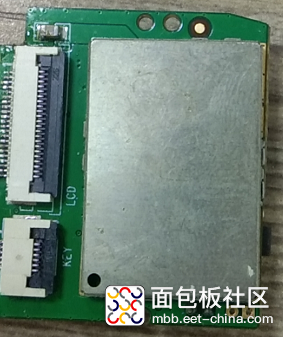
Today, electronic products generally require certification, one of which is EMC testing.EMC includes radiation testing, and to prevent radiation interference, shielding covers are often used.When asking a factory to make a shielding cover, you cannot provide them with the PCB files, so it’s best to prepare a simple dimension drawing for them. How do we create this? Let’s go through the process below.First, let’s take a look at what the shielding cover looks like, as shown in the figure: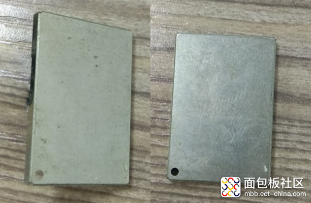 We need to extract the dimensions of the shielding cover frame from the PCB below.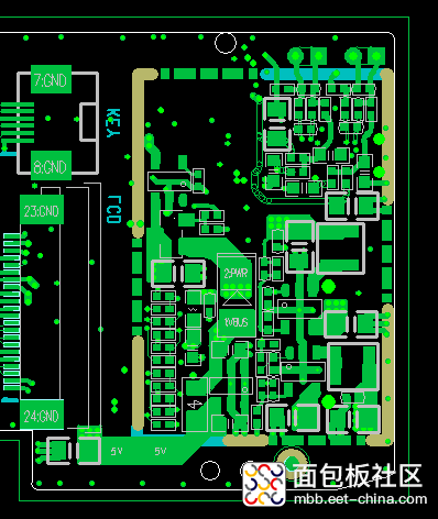
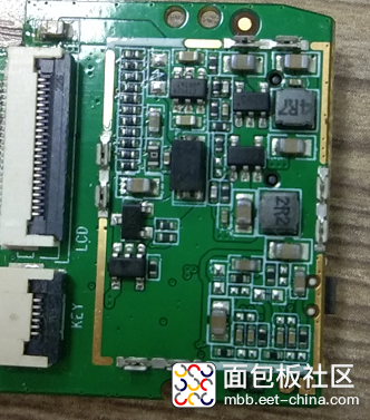 So the steps are as follows:1. Open the PCB file for the shielding cover you want to make, then select Export from the File menu to export a DXF file.
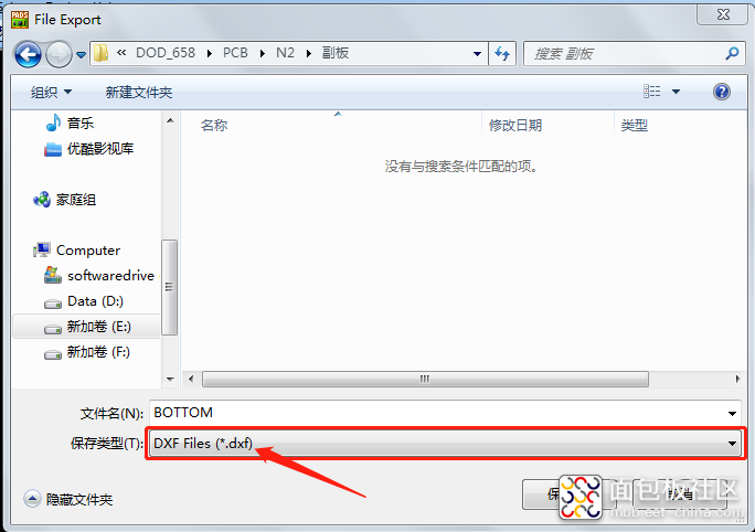
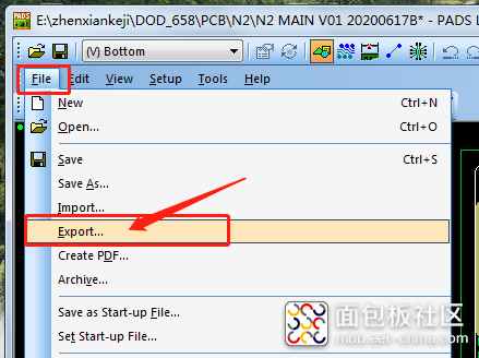 Select DXF file in the Save as type field, as indicated by the arrow in the image below:
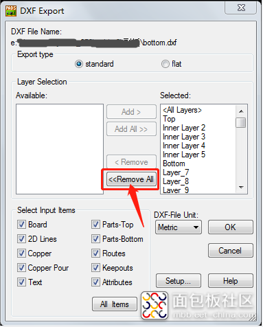
 2. After clicking Save, the export settings interface appears. By default, all layers are selected in the Selected box, so click Remove ALL to move all layers to the left, and then reselect the layers needed.
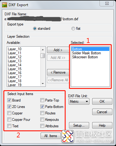
 The following image shows the state after the selection is complete. We take the shielding cover on the BOTTOM as an example, and here we can select three layers: “Bottom”, “Solder Mask Bottom”, and “Silkscreen Bottom”. Why choose these three layers?Bottom: Because the pad for the shielding cover clip is located here, it is necessary to reflect the position of the clip for making the notch later.Solder Mask Bottom: Because the window line for the contact area of the shielding cover with the PCB is drawn on this layer, this way the PCB can expose copper.Silkscreen Bottom: Because sometimes the shielding cover may press against the traces, so an additional layer of ink will be added in this area.Of course, you can set this on the Solder Mask Bottom layer, and later selecting just this layer will also work; readers can try this.The settings for the Select Input Items can be done as shown in the image below.Board: This exports the board outline, which allows you to see the entire board situation at a glance. It’s optional.2D Lines: This is the frame of the shielding cover drawn.Parts-Bottom: This exports the components on the Bottom layer; since there is a shielding cover clip, this option is selected.Once the settings are complete, click OK.
 3. Open the exported file using AUTOCAD.
 4. The effect after opening is shown below.
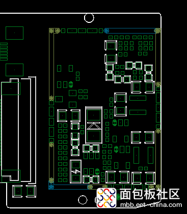 Since this is the BOTTOM layer, it needs to be mirrored, as shown in the image.
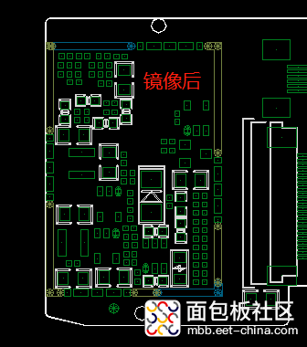 5. Delete the board outline and unused components, leaving only the shielding cover part, as shown in the image.
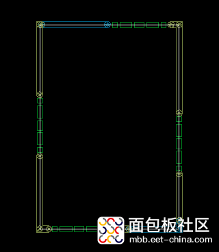
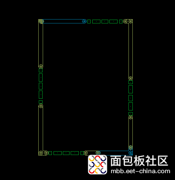 6. Draw the center line of the shielding cover frame, as shown by the white line in the image.
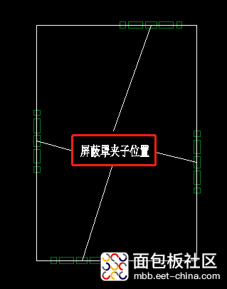
 7. Then mark the position of the shielding cover clip, as shown in the image.
 8. Make positioning holes with a diameter of about 1mm; this is to facilitate quick assembly.
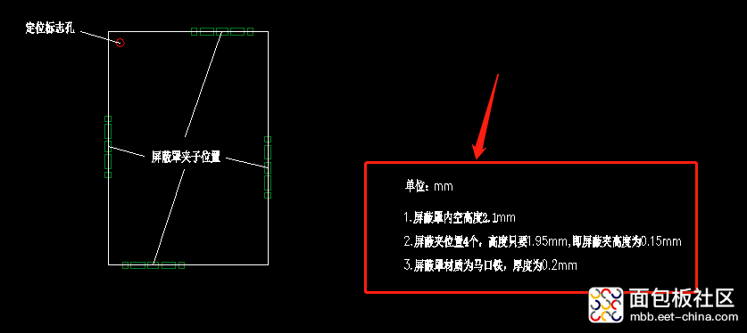
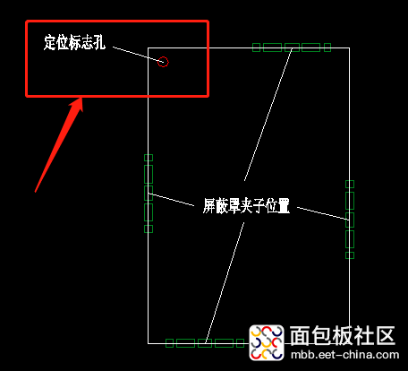 9. Write down the specifications; the internal height of the shielding cover should be about 0.1mm higher than the tallest component covered by the PCB.The thickness of the shielding cover metal is generally 0.2mm.There are two common materials for shielding covers: one is tinplate, which is relatively hard and not easy to deform, and is also relatively inexpensive, but may rust easily. The second is nickel silver, which is softer and easily deformed, but is relatively more expensive and not prone to rust.
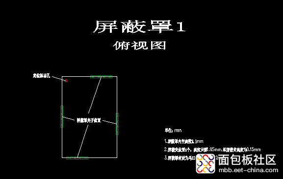
 10. Then mark the viewing angle; roughly as shown in the image, the production of the shielding cover size specification is complete.
 11. If the edges of the shielding cover press against components, notches need to be made in this part, as shown in the image.
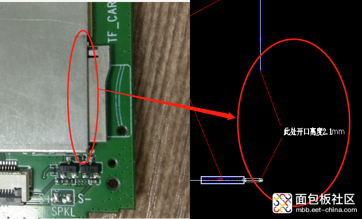 12. Below is the assembly effect after the actual production.
 Finally, I hope this explanation can be helpful to someone.Author: wuliangu, Source: Breadboard CommunityLink: https://mbb.eet-china.com/blog/uid-me-273278.htmlENDEvaluation Center Free Application


👆Long press the image to scan the code to apply👆