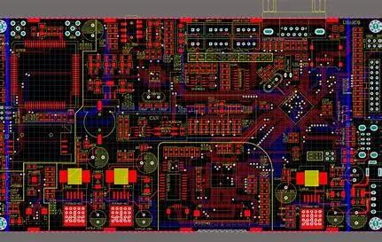
PCB Schematic
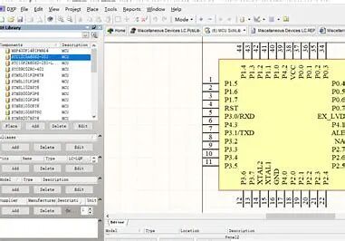
Component Library Creation
Creating a PCB schematic component library requires systematic steps and detailed operations. Below is a detailed guide:
1.Determine Requirements and Preparation
Component Information Collection: Obtain the component’s datasheet, confirm pin functions, package types (such as DIP, SMD), electrical parameters (voltage, current), etc.
Tool Selection: Choose EDA tools based on requirements, such as Altium Designer (comprehensive functionality), KiCad (open-source and free), Eagle (lightweight).
2.Create a New Component Library
Create Library File: Create a schematic library file in the EDA tool (such as Altium‘s .SchLib, KiCad‘s symbol library).
Naming Convention: Use a unified naming rule (such as manufacturer_model_package) for easier management.
3.Draw Component Symbols
Symbol Structure:
Simple Components (resistors, capacitors): Use standard symbols.
Complex ICs: Divide pins by functional modules (such as power, input/output, control).
Multi-part Components (such as 74 series logic gates): Draw in blocks for easier schematic reuse.
Pin Layout:
Functional Partitioning: Inputs on the left, outputs on the right, power/ground placed at the top and bottom.
Pin Attributes: Set numbers, names (such as VCC, GND), electrical types (Input/Output/Power, etc.).
4.Associate PCB Packages
Package Selection: Choose standard packages based on the datasheet (such as SOP16, QFN48), or create custom ones.
Pin Mapping: Ensure schematic pin numbers match package pad numbers (e.g., pin 1 corresponds to pad 1).
5.Set Component Attributes
Parameter Entry: Add model, value (such as 10kΩ), manufacturer, description, etc., for easier BOM generation.
Package Binding: Specify the associated PCB package in the schematic symbol (such as Altium‘s Footprint field).
6.Verification and Testing
DRC/ERC Check: Run design rule checks to identify unconnected pins and electrical type conflicts.
Practical Testing: Call components in a simple circuit, generate PCB and check if the netlist connections are correct.
7.Maintenance and Optimization
Version Management: Regularly update library files and annotate modification records (such as package size adjustments).
Classification Management: Store by function/manufacturer classification to improve retrieval efficiency.

Common Issues and Solutions
Pin Errors: Cross-check against the datasheet and utilize the EDA tool’s cross-probing feature.
Package Mismatch: Use the IPC package wizard or manufacturer-provided package generation tools (such as SnapEDA).
Multi-part Components: Draw in EDA tools to ensure logic gates are independently usable.
Tool Operation Example (using KiCad as an example)
1.Create Symbol: Open the symbol editor, use the rectangle tool to draw the body, add pins and set attributes.
2.Associate Package: Add package name (such as SOIC8) in the symbol properties, which must be created in the PCB package library in advance.
3.Verification: Place components in the schematic, run ERC checks, and review warnings/error messages.
Conclusion
The key to creating a component library is accuracy and standardization. Each step must strictly follow the datasheet, utilize the functions of EDA tools to simplify the process, and ensure correctness through multiple tests. Mastering these skills can significantly enhance PCB design efficiency and reliability.
END