Source: Sensor Technology
OLED (Organic Light-Emitting Diode), also known as Organic Electroluminescent Display (OELD), has been widely applied in MP3 players since 2003 due to its characteristics of being light, thin, and energy-efficient. Previously, OLED screens were only showcased as engineering samples in exhibitions for digital products like digital cameras and mobile phones, and had not yet entered practical applications. However, OLED screens possess numerous advantages over LCD that have made them highly regarded by industry professionals.
Origin of OLED Display Technology
As early as the 1960s, Pope and others first reported the electroluminescence phenomenon of anthracene single crystals, which marked the beginning of research on organic light-emitting devices. However, due to the unsatisfactory brightness and efficiency at that time, it did not attract widespread attention.
In 1987, Dr. Deng Qingyun and his team at Kodak in the USA produced multilayer devices with an electron-hole transport layer using vacuum deposition methods, achieving brightness greater than 1000 cd/㎡, efficiency exceeding 1.5 lm/W, and a driving voltage of less than 10V. These devices, characterized by their thinness, low driving voltage, self-luminescence, wide viewing angles, and fast response, garnered significant attention.
In 1990, R. H. Friend and others at the Cavendish Laboratory, University of Cambridge, prepared light-emitting devices using polymer materials, specifically poly(phenylene vinylene), as the light-emitting material, pioneering the application of polymers in organic light-emitting fields. This research further promoted the study of organic light-emitting display devices, leading to continuous reports of devices with superior performance and broader applications.
In 1993, the flexible OLED display developed by Cao Yong and others and the white OLED devices prepared by Kido and others in 1994 both had groundbreaking significance.
In 1998, researchers at Princeton University, including Forrest, incorporated phosphorescent materials into the light-emitting layer, achieving an external quantum efficiency of 5%. This research proved that OLEDs could break through the internal quantum efficiency limit of 25%, significantly improving the efficiency of organic light-emitting devices.
In 2003, Novaled produced PIN structure phosphorescent devices that improved light-emitting efficiency while enhancing charge injection capability, significantly increasing device efficiency. That same year, at the SID conference, Sony and Chi Mei launched 24-inch and 20-inch TFT OLED samples respectively, and Kodak introduced the first digital camera with an OLED display.
In May 2004, Seico Epson showcased a 40-inch color PLED panel in Japan, and Samsung SDI displayed a 17-inch OLED display screen formed by the deposition of small molecule OLED materials.
From 2005 to 2006, research focused on high-efficiency white light devices. Konica Minolta Technology Center successfully developed an OLED white light component with an initial brightness of 1000 cd/㎡, luminous efficiency of 64 lm/W, and a brightness half-life of approximately 10,000 hours.
In 2006, Samsung Electronics showcased a 2.4-inch QVGA resolution AM-OLED mobile phone screen at the IMID exhibition, while Taiwan’s Chi Mei developed a 25-inch OLED television display panel using LTPS TFT active matrix OLED technology.
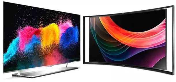
In early 2007, Chi Mei Optoelectronics officially announced mass production of AMOLED products, starting to sell small-sized (2.0-2.7 inches) displays. That same year, at the SID conference, Sony exhibited a technologically mature 11-inch OLED television.
……
Currently, over 100 research institutions and companies worldwide have invested in OLED research and production, including display giants like Samsung, LG, and Philips.
Overall, the application of OLED can be roughly divided into three stages.
1. From 1997 to 2001, the experimental stage of OLED. During this period, OLED began to gradually emerge from the laboratory, mainly applied in automotive audio panels, PDAs, and mobile phones. However, the product range was very limited, with few specifications, all being passive-driven, monochrome or area color, largely experimental and trial sales in nature. In 2001, the global sales of OLED were only about $150 million.
2. From 2002 to 2005, the growth stage of OLED. During this period, people began to gradually encounter more products with OLED, such as in-car displays, PDAs, mobile phones, digital cameras, DCs, head-mounted displays, etc. However, the focus was mainly on small panels under 10 inches, while panels over 10 inches began to be used.
3. After 2005, OLED entered a matured stage. After 2008, this maturation will accelerate, with technology and market advancing rapidly under market drive. Large size and lifespan will become the main breakthrough directions for OLED technology in the future.
Basic Structure and Principle of OLED
The basic structure of OLED consists of a thin, transparent, semiconductor-like indium tin oxide (ITO), connected to the positive electrode of the power supply, along with another metal cathode, forming a sandwich structure. The entire structure layer includes: Hole Transport Layer (HTL), Emission Layer (EL), and Electron Transport Layer (ETL). When power is supplied at an appropriate voltage, holes from the positive electrode and charges from the cathode combine in the emission layer, producing light in red, green, and blue (RGB) primary colors depending on their formulation.
The characteristic of OLED is its self-luminescence, unlike TFT LCDs that require backlighting, thus providing high visibility and brightness. Additionally, it has low voltage requirements and high energy efficiency, along with fast response, lightweight, thinness, simple structure, and low cost, making it one of the most promising products of the 21st century.
The basic structure of OLED is shown in the figure. It consists of the following parts:
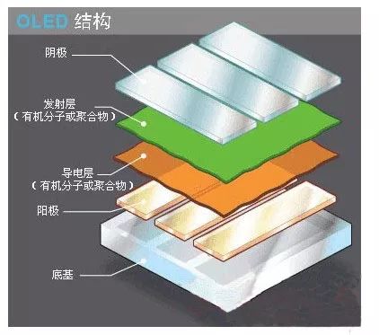
Substrate (transparent plastic, glass, metal foil) – The substrate supports the entire OLED.
Anode (transparent) – The anode eliminates electrons (increases “holes”) when current flows through the device.
Organic Layer – The organic layer is composed of organic molecules or organic polymers.
Conductive Layer – This layer is composed of organic plastic molecules that transport the “holes” from the anode. Conductive polymers like polyaniline can be used as the conductive polymer for OLED.
Emission Layer – This layer is composed of organic plastic molecules (distinct from the conductive layer) that transport electrons from the cathode; the light-emitting process occurs in this layer. Polyfluorene can be used as the polymer for the emission layer.
Cathode (can be transparent or opaque, depending on the type of OLED) – When current flows through the device, the cathode injects electrons into the circuit.
The light-emitting process of OLED typically occurs in five stages:
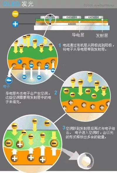
1. Injection of charge carriers under the influence of an external electric field: electrons and holes are injected from the cathode and anode, respectively, into the organic functional thin film sandwiched between the electrodes.
2. Migration of charge carriers: The injected electrons and holes migrate from the electron transport layer and hole transport layer to the emission layer.
3. Recombination of charge carriers: Electrons and holes recombine to generate excitons.
4. Migration of excitons: Under the influence of the electric field, excitons migrate, transferring energy to light-emitting molecules and exciting electrons from the ground state to the excited state.
5. Electroluminescence: The energy of the excited state is released through radiative transitions, producing photons and releasing energy.
Methods for Colorization of OLED
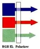
RGB pixel independent light emission
The use of independent light-emitting materials is currently the most widely used color mode. It utilizes precise metal masks and CCD pixel alignment technology to first prepare red, green, and blue primary color light-emitting centers, then adjusts the mixing ratio of the three colors to produce true colors, allowing the three-color OLED components to emit light independently to form a pixel. The key to this technology lies in enhancing the color purity and luminous efficiency of the light-emitting materials, while the metal mask etching technology is also crucial.
Currently, organic small molecule light-emitting material AlQ3 is a very good green light-emitting small molecule material, with excellent green light color purity, luminous efficiency, and stability. However, the best red light-emitting small molecule material for OLED has a luminous efficiency of only 31 m/W and a lifespan of 10,000 hours, while the development of blue light-emitting small molecule materials is also slow and challenging. The greatest bottleneck faced by organic small molecule light-emitting materials lies in the purity, efficiency, and lifespan of red and blue materials. However, through doping the main light-emitting materials, researchers have achieved relatively good color purity, luminous efficiency, and stability for blue and red light.
The advantage of polymer light-emitting materials is that their light-emitting wavelength can be adjusted through chemical modification, achieving a range of colors covering the entire visible spectrum from blue to green to red. However, their lifespan is only one-tenth of that of small molecule light-emitting materials, so improvements in luminous efficiency and lifespan of polymer light-emitting materials remain necessary. Continuously developing high-performance light-emitting materials should be a challenging and long-term task for material developers.
With the colorization, high resolution, and large area of OLED displays, the metal mask etching technology directly affects the quality of the display panel, thus imposing more stringent requirements on the precision of the metal mask pattern size and positioning accuracy.
Color Conversion
Color conversion involves combining blue OLED with a color conversion film array, first preparing devices that emit blue light from OLED, then using this blue light to excite color conversion materials to obtain red and green light, thus achieving full color. The key to this technology is to enhance the color purity and efficiency of the color conversion materials.
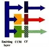
This technology does not require metal mask alignment technology, only the deposition of blue OLED components, making it one of the most promising full-colorization technologies for large-size full-color OLED displays. However, its drawback is that the color conversion materials easily absorb blue light from the environment, causing a decrease in image contrast, while light guiding can also lead to a reduction in image quality. Currently, this technology is mastered by Japan’s Idemitsu Kosan Company, which has produced a 10-inch OLED display.
Color Filter Film
This technology uses white OLED combined with a color filter film, first preparing devices that emit white light from OLED, then obtaining the three primary colors through the color filter film, and finally combining the three primary colors for color display.
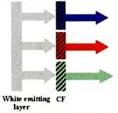
The key to this technology is obtaining high efficiency and high purity white light. Its manufacturing process does not require metal mask alignment technology and can utilize the mature color filter film manufacturing technology used in LCD displays. Therefore, it is one of the promising full-colorization technologies for large-size full-color OLED displays. However, using this method results in light loss of up to two-thirds due to the color filter film. Currently, Japan’s TDK and America’s Kodak companies are using this method to produce OLED displays.
RGB pixel independent light emission, color conversion, and color filter film are three manufacturing technologies for the full-colorization of OLED displays, each with its advantages and disadvantages, depending on the process structure and organic materials used.
Characteristics of OLED Technology
1. Light and thin: Ultra-thin is a trend in mobile phone development, which presents a huge opportunity for OLED, known for its lightweight and thin characteristics.
2. Fast response speed: The response speed of OLED is more than 1000 times faster than that of LCD, with no image trailing phenomenon, making it particularly suitable for 3G video technology.
3. Good stability: Within the operating temperature range, the stability of OLED’s optoelectronic parameters is very good. LCDs, due to the inherent properties of liquid crystals at high and low temperatures, usually dim at low temperatures and slow down their response speed, while brightening at high temperatures. However, OLED maintains its contrast, response speed, and brightness within its allowable operating range.
4. Short lifespan: The working lifespan of OLED is usually defined as the duration until the brightness decreases to 50% of its initial brightness while still functioning. Currently, many OLED manufacturers can only guarantee a product lifespan of around 8000 hours. This is mainly due to the decay of organic light-emitting materials, so developing long-lifespan light-emitting materials is an urgent task.
5. High power consumption: Currently, the power consumption of OLED is several times that of an equivalent-sized LCD. Developing high luminous efficiency organic materials and new driving methods is fundamental to solving this problem.
6. Image retention: Due to brightness decay, pixels that are continuously illuminated will have residual images.
7. Poor outdoor visibility: Since OLED is self-luminous, its visibility is poor under strong sunlight outdoors. The only way to solve this problem is to increase surface brightness and contrast.
Driving of OLED Circuits
Based on the relationship between the driving circuit and the substrate, OLEDs are divided into two categories: active matrix and passive matrix organic light-emitting displays.
For passive matrix organic light-emitting displays
These displays require external driving circuits around the substrate. The display area on the display substrate consists solely of light-emitting pixels (electrodes, functional layers), and all driving and control functions are completed by integrated ICs (which can be placed outside the substrate or in the non-display area of the substrate). The driving method for passive matrices is multi-channel dynamic driving, which is limited by the number of scanning electrodes, and the duty cycle coefficient is an important parameter for passive driving.
For active matrix organic light-emitting displays
These displays integrate external driving circuits and display arrays on the same substrate. Within the display area on the display substrate, each pixel is equipped with at least two thin-film transistors and one charge storage capacitor, ensuring that the state of each pixel’s light emission remains unchanged during the scanning addressing of a field.
Static driving
Each organic electroluminescent pixel’s common electrode (e.g., cathode) is connected together, while the other electrode (e.g., anode) is separately connected. The voltage applied to the discrete electrodes determines whether the corresponding pixel emits light. During the display cycle of an image, the state of pixel emission remains unchanged.
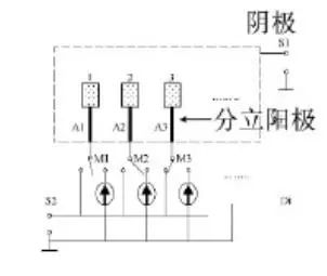
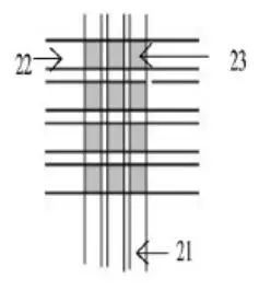
Dynamic driving
The two electrodes of the pixels on the display are structured in a matrix format, meaning that the same nature of horizontal display pixels shares the same electrode, while the same nature of vertical display pixels shares another electrode. If the pixels can be divided into N rows and M columns, there will be N row electrodes and M column electrodes, referred to as row and column electrodes respectively. To illuminate all pixels on the screen, either a row-by-row or column-by-column illumination method is adopted, with the time to illuminate all pixels being less than the human eye’s visual retention limit of 20 ms.
Active matrix driving is a static driving method, where active matrix OLEDs have a storage effect and can perform 100% load driving. This driving is not limited by the number of scanning electrodes and allows for selective adjustment of each pixel independently.
Active matrix can achieve high brightness and high resolution. Passive matrix faces duty cycle issues, where non-selected displays quickly fade away. To achieve a certain brightness level on the display, the brightness during scanning of each column must equal the average brightness of the screen multiplied by the number of columns. For example, with 64 columns, if the average brightness is 100 cd/㎡, then the brightness of one column should be 6400 cd/㎡. As the number of columns increases, the brightness of each column must also increase, consequently requiring an increase in driving current density. Thus, it is evident that passive matrix struggles to achieve high brightness and high resolution. Active matrix does not face duty cycle issues, is not limited by the number of scanning electrodes, and is easier to achieve high brightness and high resolution. Active driving also has many other advantages, such as increased luminous brightness, reduced power consumption of electrode leads, improved uniformity and lifespan, making large-area high-resolution displays possible.
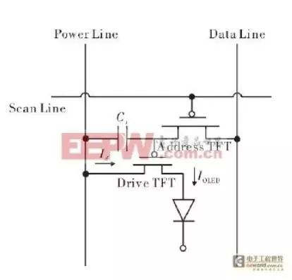
For the implementation of the OLED driving control system, the key technology lies in data writing and scanning control. The above diagram shows the dual-tube driving circuit for a single pixel. One TFT is used for addressing, while the other is a current modulation transistor used to supply current to the OLED. To prevent variations in the opening voltage of the OLED from causing current changes, a P-channel device is used, ensuring that the OLED is driven by the drain of the driving TFT, making the source voltage independent of the voltage on the organic layer. The Data Line is connected to the source of the addressing TFT, and the Scan Line enables the addressing TFT. The content on the data line is written to the storage capacitor (CS) in the form of charge and temporarily stored. When the Power Line is at a high level, the source of the driving TFT is also at a high level, and the charge on the CS will enable the driving TFT, allowing its drain current to flow through the OLED display device, driving it to emit light. The level of the data line determines the brightness or darkness of the pixel.
Methods for Modulating Gray Scale Display in OLED
Amplitude Modulation Method
OLED is a current-driven device, where brightness is proportional to current density. When the light-emitting area is constant, brightness is proportional to current. Gray scale display is achieved by modulating the current amplitude.
Spatial Modulation Method
The basic principle is to divide each pixel into several sub-pixels, where the gray level of each pixel is determined by the number of sub-pixels that are illuminated. In this method, the specific implementation involves defining a display unit on the OLED display screen as a collection of many sub-units, which can be independently controlled; when different numbers of sub-units within that unit are enabled, corresponding gray levels will be achieved; the display pixels composed of different combinations of enabled sub-pixels will show different gray levels.
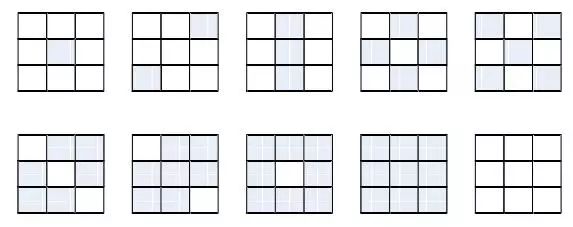
This method exchanges a decrease in resolution and an increase in fine processing costs for a certain gray level. To maintain the original resolution, further segmentation and processing of the original sub-pixels will be very challenging.
Time Modulation Method
Within a short time frame, the human eye’s perception of brightness depends on the intensity of the light-emitting object and the duration for which the light-emitting body is illuminated; the longer the illumination time, the stronger the human eye’s perception of the light intensity, presenting an effect similar to integration. It is one of the commonly used gray scale display solutions, mainly including pulse width modulation and sub-field modulation.
Pulse Width Modulation Method
Pulse width modulation divides the row scanning cycle into segments. For example, to achieve 16 levels of gray scale display, the row scanning cycle can be further divided into 16 sub-segments. In each sub-segment, the column electrodes apply conducting/disconnecting voltage in a specific time ratio. When all sub-segments are applied with conducting voltage, the unit is in an enabled state, achieving the highest brightness level; conversely, when all are disconnected, the unit is in a non-enabled state, achieving the lowest brightness level; when some sub-segments are in the conducting state while others are in the disconnecting state, different gray levels can be achieved based on the duration of conduction and disconnection. Thus, when the time of each sub-segment is very small, high gray levels can be displayed. Its drawbacks include complex timing relationships, high circuit overhead, and limitations due to the OLED display’s inability to respond to excessively narrow pulse width values.
Sub-field Modulation Method
Sub-field modulation is also a time gray modulation method. As previously mentioned, within a certain time frame, the longer the illumination time, the stronger the human eye’s perception of light intensity. The sub-field modulation technique utilizes this visual retention characteristic to divide the OLED’s illumination time into several sub-fields, distinguishing brightness through varying illumination times to achieve gray scale display.
By treating the OLED’s light-emitting unit as having only two states: “off” and “on,” the display time of the input signal within a frame is divided in a ratio of 1:2:4:8… into several sub-fields. By combining the sub-fields, any level of gray scale display corresponding to the pixel’s illumination time can be achieved, thereby achieving gray scale display for OLED. For full-color OLED displays, the RGB three-color pixels only need to be driven in their respective ways and then combined on the screen.
Types of OLED
The main types of OLED include: Passive Matrix OLED (PMOLED), Active Matrix OLED (AMOLED), Transparent OLED, Top Emission OLED, Foldable OLED, White OLED, etc.
Passive Matrix OLED (PMOLED)
PMOLED consists of cathode strips, organic layers, and anode strips. The anode strips and cathode strips are perpendicular to each other. The intersection of the cathode and anode forms pixels, which are the emitting parts. External circuits apply current to selected cathode and anode strips, determining which pixels emit light and which do not. Additionally, the brightness of each pixel is proportional to the magnitude of the applied current.
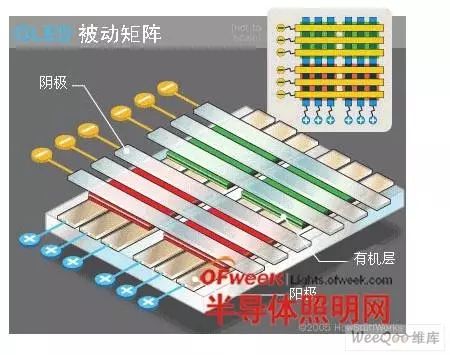
PMOLED is easy to manufacture but consumes more power than other types of OLED, mainly due to the need for external circuits. PMOLED is most efficient when used to display text and icons, suitable for making small screens (diagonal 2-3 inches), such as those commonly seen on mobile phones, handheld computers, and MP3 players. Even with an external circuit, the power consumption of passive matrix OLED is still lower than that of the LCDs currently used in these devices.
Active Matrix OLED (AMOLED)
AMOLED features a complete cathode layer, organic molecular layer, and anode layer, but the anode layer is covered with a thin-film transistor (TFT) array, forming a matrix. The TFT array itself is a circuit that can determine which pixels emit light, thus determining the composition of the image.
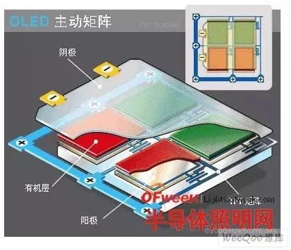
AMOLED consumes less power than PMOLED, as the power required for the TFT array is less than that of external circuits, making AMOLED suitable for large display screens. AMOLED also has a higher refresh rate, making it suitable for displaying videos. The best applications for AMOLED are computer monitors, large-screen televisions, and electronic billboards or displays.
Transparent OLED
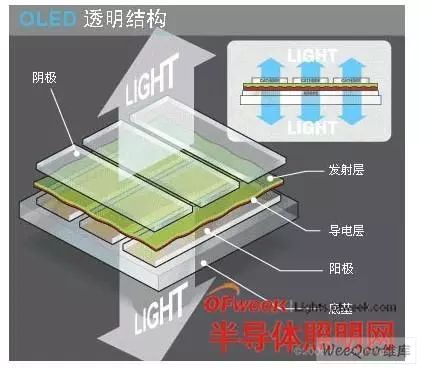
Transparent OLED only contains transparent components (substrate, anode, cathode), achieving a maximum transparency of 85% when not emitting light. When the transparent OLED display is powered, light can pass through in both directions. Transparent OLED displays can use either passive or active matrix designs. This technology can be used to create head-up displays commonly used in aircraft.
Top Emission OLED
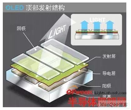
Top emission OLED has opaque or reflective substrates. They are best suited for active matrix designs. Manufacturers can use top emission OLED displays to create smart cards.
Foldable OLED
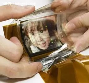
Foldable OLED has a substrate made of flexible metal foil or plastic. Foldable OLEDs are lightweight and very durable. They can be used in devices such as mobile phones and handheld computers, effectively reducing the rate of device damage, which is a major cause of returns and repairs. In the future, foldable OLEDs may be stitched into fibers to create “smart” clothing. For example, future survival suits could integrate computer chips, mobile phones, GPS receivers, and OLED displays sewn into the fabric.
White OLED
White OLED emits white light that is brighter, more balanced, and more energy-efficient than the white light emitted by fluorescent lamps. White OLED also possesses the true color characteristics of incandescent lighting. We can make OLED into large, thin sheets, allowing OLED to replace the fluorescent lamps currently used in homes and buildings. In the future, using OLED is expected to reduce the energy consumption required for lighting.
Main Parameters for Evaluating OLED Performance
Generally, the performance of OLED light-emitting materials and devices can be evaluated from two aspects: light-emitting performance and electrical performance. Light-emitting performance mainly includes emission spectrum, luminous brightness, luminous efficiency, colorimetry, and lifespan; while electrical performance includes the relationship between current and voltage, and the relationship between luminous brightness and voltage, all of which are key parameters for measuring OLED material and device performance.
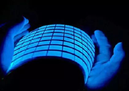
Emission Spectrum
The emission spectrum refers to the relative intensity of various wavelength components in the emitted fluorescence, also known as the distribution of relative intensity of fluorescence with respect to wavelength. The emission spectrum is generally measured using various models of fluorescence measurement instruments, where the fluorescence is irradiated through a monochromatic emitter onto a detector, scanning the monochromatic emitter and detecting the corresponding fluorescence intensity at various wavelengths, then recording the fluorescence intensity against the emission wavelength relationship curve to obtain the emission spectrum.
The emission spectrum of OLED has two types: photoluminescence (PL) spectrum and electroluminescence (EL) spectrum. The PL spectrum requires optical energy excitation, maintaining the wavelength and intensity of the excitation light; the EL spectrum requires electrical energy excitation, and can be measured under different voltage or current density conditions. By comparing the EL spectrum of the device with the PL spectrum of different carrier transport materials and light-emitting materials, the position of the composite region and useful information about the actual light-emitting substance can be derived.
Luminous Brightness
The unit of luminous brightness is cd/㎡, indicating the light intensity per square meter. Luminous brightness is generally measured using a brightness meter. The brightness of the earliest OLED devices has exceeded 1000 cd/㎡, while the brightest OLEDs currently can exceed 140,000 cd/㎡.
Luminous Efficiency
The luminous efficiency of OLED can be expressed in terms of quantum efficiency, power efficiency, and lumen efficiency. Quantum efficiency ηq refers to the ratio of the number of output photons Nf to the number of injected electron-hole pairs Nx. Quantum efficiency is further divided into internal quantum efficiency ηqi and external quantum efficiency ηqe. Internal quantum efficiency ηqi is the ratio of the number of photons produced by recombination within the device to the number of injected electron-hole pairs; in fact, the luminous efficiency of the device is reflected by external quantum efficiency ηqe, which can be expressed by the following equation. External quantum efficiency can be measured using an integrating sphere photometer to measure the total luminous flux of the light-emitting device per unit time, deriving the external quantum efficiency of the device through calculations. The energy of the excitation light photons is always greater than that of the emitted light photons. When the excitation light wavelength is significantly shorter than the emitted light wavelength, this energy loss can be considerable, and quantum efficiency cannot reflect this energy loss, necessitating the use of power efficiency to reflect it. Power efficiency ηp, also known as energy efficiency, refers to the ratio of output optical power Pf to input electrical power Px. When assessing the functionality of a light-emitting device, the lumen efficiency parameter is often used. Lumen efficiency ηl, also known as luminous efficiency, is the emitted luminous flux L (in lumens) divided by the input electrical power Px. Here, S is the emission area (㎡), B is the luminous brightness (cd/㎡), I and V are the bias current and voltage applied when measuring brightness, and J is the corresponding current density (A/㎡). The unit of lumen efficiency is lm/W.
Luminous Colorimetry
Luminous colorimetry is represented by color coordinates (x, y, z), where x represents the red value, y represents the green value, and z represents the blue value. Typically, the color can be represented by the two color coordinates x and y.
Luminous Lifespan
Lifespan refers to the time required for brightness to decrease to 50% of its initial brightness. Commercially available OLED devices are required to have a continuous lifespan of over 10,000 hours, with a storage lifespan requirement of 5 years. Research has found that one of the factors affecting the lifespan of OLED devices is the presence of water and oxygen molecules, so it is essential to isolate them during device packaging.
Current Density – Voltage Relationship
In OLED devices, the curve reflecting the change in current density with voltage reveals the electrical properties of the device, resembling the current density-voltage relationship of light-emitting diodes, exhibiting rectifying effects. At low voltages, the current density increases slowly with increasing voltage, while beyond a certain voltage, the current density rises sharply.
Luminosity – Voltage Relationship
The luminosity-voltage relationship curve reflects the optical properties of OLED devices, similar to the current-voltage relationship curve of the device, indicating that at low driving voltages, current density and brightness increase slowly, while at high voltage driving, brightness increases rapidly alongside a sharp increase in current density. The luminosity-voltage relationship curve can also provide information about the starting voltage, which is defined as the voltage at which brightness reaches 1 cd/㎡.
– END –
Editor: Southern Cat