1 Photoresist: The Core Material Needed for Photolithography Process, Supporting Continuous Process UpgradingThe century-long development history of photoresist is a key material required for photolithography processes. Photoresist has been applied in the printing industry for over a century. By the 1920s, it began to be used in the PCB field, and in the 1950s, it started to be used in wafer production. In the late 1950s, Eastman Kodak and Shipley (now acquired by Dow) designed positive and negative photoresists suitable for the semiconductor industry. Photoresist is used in the photolithography process to help transfer designed circuit patterns from masks to silicon wafers, thereby achieving specific functions. The quality and performance of photoresist directly affect the yield of manufacturing production lines.For example, in integrated circuits, the steps of the photolithography process and the usage scenarios of photoresist are as follows:1) Pre-treatment of the silicon wafer surface: Before lithography, the wafer undergoes a wet cleaning and deionized water rinse to remove contaminants. After cleaning, the wafer surface needs to undergo hydrophobic treatment to enhance the adhesion of the photoresist (which is usually hydrophobic) to the wafer surface.2) Spin coating of photoresist and anti-reflective layer: After gas pre-treatment, the photoresist needs to be applied to the wafer surface. The most widely used method of application is the spin coating method, where approximately a few milliliters of photoresist are delivered to the center of the wafer, and then the wafer is spun up and gradually accelerated until it stabilizes at a certain rotational speed (the speed determines the thickness of the resist, which is inversely proportional to the square root of the speed).3) Pre-exposure baking: Once the photoresist is spun on the wafer surface, it must undergo baking. The purpose of baking is to drive away almost all solvents. This baking, which occurs before exposure, is called “pre-exposure baking,” or “soft bake.” Pre-baking improves the adhesion of the photoresist, enhances its uniformity, and controls the width uniformity during the etching process.4) Alignment and exposure: In projection exposure methods, the mask is moved to a predetermined approximate position on the wafer or to the appropriate position relative to the existing patterns on the wafer, and then the pattern is transferred to the wafer through photolithography by the lens. In proximity or contact exposure, the pattern on the mask is directly exposed to the wafer by the ultraviolet light source.5) Post-exposure baking: After exposure, the photoresist needs to undergo another baking process. The purpose of post-baking is to fully complete the photochemical reaction through heating. The photosensitive components generated during the exposure process will diffuse under the heat and chemically react with the photoresist, changing the previously almost insoluble photoresist material in the developing liquid into a material that is soluble in the developing liquid, forming a pattern of soluble and insoluble areas in the photoresist film. Since these patterns are consistent with those on the mask but have not been displayed, they are also called “latent images.”6) Development: Since the photoresist after photochemical reaction is acidic, the developing solution uses a strong alkaline solution. Typically, a 2.38% aqueous solution of tetramethylammonium hydroxide is used. After the development process, the exposed areas of the photoresist are washed away by the developing solution, and the pattern on the mask is displayed on the photoresist film on the wafer in a shape with or without photoresist.7) Hard bake: After development, since the wafer comes into contact with moisture, the photoresist will absorb some moisture, which is detrimental to subsequent processes such as wet etching. Therefore, a hard bake is required to expel excessive moisture from the photoresist. Since most etching is now done using plasma etching, also known as “dry etching,” hard baking has been omitted in many processes.8) Measurement: After exposure, it is necessary to measure the critical dimensions and overlay accuracy formed by the lithography. The measurement of critical dimensions usually uses scanning electron microscopes, while the measurement of overlay accuracy is undertaken by optical microscopes and charge-coupled device imaging detectors.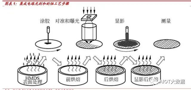 Process upgrading determines the development direction, and lithography equipment and photoresist are core factors. With the development of high integration, ultra-high speed, and ultra-high frequency integrated circuits and components, the feature sizes of integrated circuits and components are showing an increasingly fine trend, with processing sizes reaching hundreds of nanometers down to the nanoscale. Lithography equipment and photoresist products are also being continuously innovated to meet the processing applications of ultra-fine electronic circuit patterns. The resolution of photoresist directly determines the size of the feature dimensions; generally, the shorter the exposure wavelength, the higher the resolution. Therefore, to adapt to the continuously shrinking requirements of integrated circuit line widths, the exposure wavelengths of photoresist have shifted from ultraviolet broad spectrum to g-line (436nm) → i-line (365nm) → KrF (248nm) → ArF (193nm) → F2 (157nm), and the resolution level of photoresist is continuously enhanced through resolution enhancement technologies.
2 A Global Market Worth Billions, Driven by Display + PCB + IC Applications
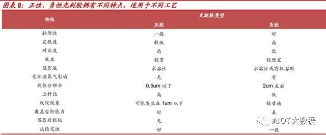
The global market continues to expand, with expectations to exceed 10 billion USD in 2023. As a critical raw material for manufacturing, the photoresist market is expected to continue growing with the rapid development of fields such as automotive, artificial intelligence, and national defense. According to Reportlinker data, the global photoresist market is expected to achieve a compound annual growth rate (CAGR) of 6.3% from 2019 to 2026, breaking through 10 billion USD by 2023 and exceeding 12 billion USD by 2026.The mainland market’s growth rate is higher than the global average, with expectations to exceed 10 billion RMB in 2022. Coupled with industrial transfer factors, the growth rate of China’s photoresist market has outpaced the global average. According to data from the China Business Industry Research Institute, the Chinese photoresist market reached 9.33 billion RMB in 2021, with a CAGR of 11.9% from 2016 to 2021, and a year-on-year growth of 11.7% in 2021, higher than the global growth rate of 5.75% during the same period. As the PCB, LCD, and semiconductor industries continue to transfer to China, the Chinese photoresist market is expected to continue expanding, and its share of the global photoresist market is expected to increase from around 15% in 2019 to 19.3% by 2026.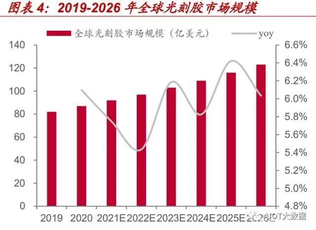 Displays, PCBs, and ICs are the three major application areas, accounting for over 70% combined. Depending on the application field, photoresists can be divided into photoresists for printed circuit boards (PCBs), liquid crystal displays (LCDs), semiconductors, and other uses. According to Reportlinker data, in 2019, the shares of PCB, semiconductor, and flat panel display photoresists were 27.8%, 21.9%, and 23.0%, respectively, making them the top three application areas.Based on whether the exposed area is removed or retained during the development process, photoresists are divided into positive photoresists (positive resists) and negative photoresists (negative resists). Each type has its advantages, but positive resists have higher resolution and are the mainstream type. 1) Positive photoresist: Under exposure from ultraviolet and other light sources, the pattern is transferred to the photoresist coating, and the exposed parts undergo a decomposition reaction, becoming soluble in the developing solution, while the unexposed parts remain on the substrate, replicating the same pattern as on the mask. Positive photoresists respond to wavelengths of 330 to 430 nanometers, with film thickness of 1 to 3 microns, and they have higher resolution without swelling. Therefore, the application of positive photoresists is more widespread than that of negative photoresists. 2) Negative photoresist: Under exposure from ultraviolet and other light sources, the pattern is transferred to the photoresist coating, and under the action of the developing solution, the exposed parts of the negative photoresist undergo a cross-linking reaction and become insoluble in the developing solution; the unexposed parts dissolve in the developing solution, replicating the opposite pattern from the mask onto the substrate. Negative photoresists respond to wavelengths of 330 to 430 nanometers, with film thickness of 0.3 to 1 microns, and their resolution is lower than that of positive photoresists.Negative resists account for a smaller proportion of total photoresists and are mostly used in special processes. Due to their strong heat resistance, negative resists are often used in high-power devices and high-energy-consuming devices, and they are also commonly used in some special processes, as their difficult removal characteristics allow them to be used in the final packaging stage of chips, providing insulation and protection for the chips.In summary, positive resists have the following main advantages: 1) High resolution and contrast; 2) Using dark field masks reduces the defect rate of the exposed pattern, as most areas of the mask are opaque; 3) Use of water-soluble developing solutions; 4) Easy to remove. Therefore, the prevalence of positive resists is greater than that of negative resists.
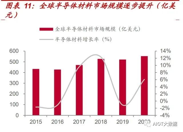
 2.1 Semiconductor Photoresists: The Highest Technical Difficulty and Fastest GrowthThe global semiconductor photoresist market is growing at a rate far exceeding the average level of the global photoresist market, with its share continuously increasing. According to SEMI statistics, the global semiconductor photoresist market reached 2.471 billion USD in 2021, a year-on-year growth of 19.49%. From 2015 to 2021, the CAGR was 12.03%. In 2019, the global semiconductor photoresist market was approximately 1.8 billion USD, accounting for about 21.9% of the overall photoresist market, which increased to 26.85% by 2021.The growth rate of semiconductor photoresists in mainland China is more than twice that of the global rate. Regionally, the semiconductor photoresist market in mainland China maintained the fastest growth rate, reaching 493 million USD in 2021, a year-on-year increase of 43.69%, more than double the overall growth rate of semiconductor photoresists for the year; China’s share of the global semiconductor photoresist market is expected to rise from approximately 10.4% in 2015 to nearly 20% in 2021.
 The rapid rise of China’s semiconductor photoresists is inseparable from the overall development of China’s semiconductor industry. Benefiting from the large-scale construction of 5G and the widespread adoption of remote work and online streaming applications due to the COVID-19 pandemic, the global integrated circuit industry has developed rapidly. According to Frost & Sullivan data, in 2013, the integrated circuit market size was 251.8 billion USD, reaching 333.4 billion USD in 2019, with a CAGR of 4.79%. The global integrated circuit market saw a decline in 2019, mainly due to global trade frictions, fluctuations in supply and demand for memory, and declining demand for products such as smartphones and servers. By 2025, the global integrated circuit market is expected to reach 475 billion USD, with a CAGR of 6.02% from 2020 to 2025.China’s integrated circuit industry started relatively late but has developed rapidly. According to the China Semiconductor Industry Association, in 2013, China’s integrated circuit sales revenue was 250.8 billion RMB, reaching 756.2 billion RMB in 2019, with an average CAGR of 20.2%. Driven by the development of 5G and emerging industries, such as the automotive electronics industry and the Internet of Things, the market size of China’s integrated circuit industry is expected to continue expanding, with an expected market size of 1,893.2 billion RMB by 2025, with a CAGR of 16.22% from 2020 to 2025.In terms of exposure wavelengths, the global market for ArF/EUV photoresists accounts for over 50%, making them the mainstream in the international market. Semiconductor photoresists can be divided into five categories based on exposure wavelengths: g-line (436nm), i-line (365nm), KrF (248nm), ArF (193nm), and the emerging EUV photoresists. High-end photoresists refer to KrF, ArF, and EUV photoresists, with higher resolution limits and greater wiring density on the same area of silicon wafers, resulting in better performance. According to TECHCET data, from the market distribution perspective, in 2021, ArFi+ArF photoresists accounted for 48.1% of the global photoresist market size, while KrF accounted for 34.7%, and G/I lines accounted for 14.7%. ArF (including ArFi) photoresists have become the most demanded photoresist products in integrated circuit manufacturing, and with the continuous development of ultra-advanced processes in the integrated circuit industry, ArF photoresists are continuously welcoming vast market opportunities.
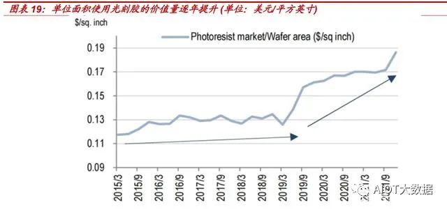
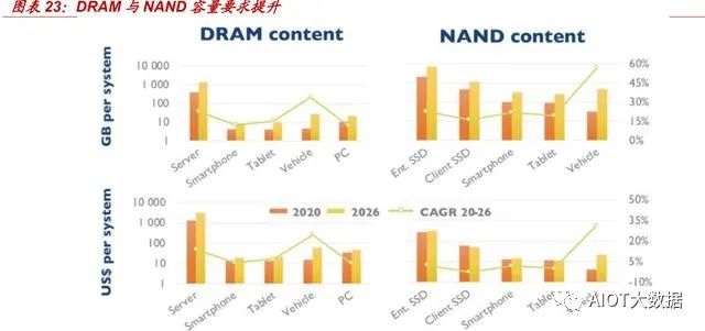
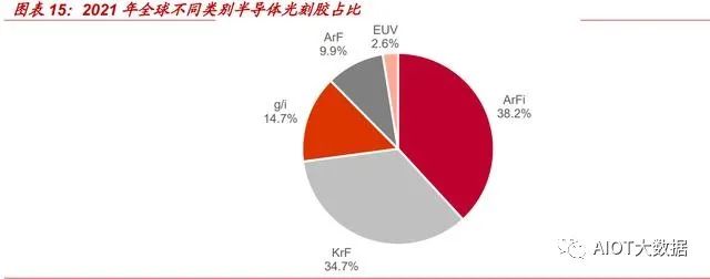 With the development of the global semiconductor industry and the continuous reduction of manufacturing process technology nodes, the demand for KrF and ArF photoresists is increasing significantly, and they are the main factors driving the rapid growth of the current photoresist market. From the perspective of market growth, EUV photoresists are developing the fastest, but their volume is relatively small in the early stages of development. In 2021, the market size was only about 51 million USD, and it is expected to reach 197 million USD by 2025, with a CAGR of 48.8% from 2020 to 2025. The second fastest growth is KrF photoresists, whose global market size in 2021 was 690 million USD, and it is expected to reach 907 million USD by 2025, with a CAGR of 8.2% from 2020 to 2025. ArF photoresists (ArF+ArFi) had a global market size of 955 million USD in 2021, expected to reach 1.072 billion USD by 2025, with a CAGR of 3.5% from 2020 to 2025. The lower-end g/i line photoresists are expected to see little change in market size, with a shrinking share.From the perspective of application products, in 2021, logic accounted for over 63.5%, making it the largest application area. Non-volatile memory (NVM) is a type of memory that can retain saved data even when the computer is powered off, and it is experiencing the fastest growth. According to TECHCET data, in 2021, the demand for logic photoresists exceeded 5.95 million liters, accounting for over 63.5%, and by 2025, the demand is expected to increase to approximately 6.77 million liters. The CAGR from 2021 to 2025 is 3.3%, and due to the rapid increase in demand for photoresists for NVM (with a CAGR of 12.8% from 2021 to 2025), it is expected that by 2025, the logic share will slightly decrease to 59.5%, while the NVM share will increase to 26.4%. The demand for non-volatile memory (NVM) is mainly due to the significant increase in storage capacity required by mobile devices, especially in cameras, smartphones, and tablets.As the process shrinks and storage capacity increases, the number of lithography steps increases, and the amount of photoresist used per unit area increases. According to SEMI data, the value of photoresist used per unit area has risen from less than 0.12 USD/sq.in in March 2015 to approximately 0.19 USD/sq.in in September 2021. The increase in average value is mainly due to the increase in the proportion of advanced processes and the increase in the number of lithography steps.
 Logic: Process Upgrading + Capacity Expansion Are the Two Major Driving ForcesThe more advanced the process, the more lithography steps are required, and the amount of photoresist used increases accordingly. To achieve the required narrower line widths and break through the line width limit, key layers of high-end processes require double or even multiple exposures. With the increase in the number of exposures, the demand for photoresist is also rapidly increasing. For example, the 28nm process requires only 6 lithography steps, while the 7nm immersion lithography requires 34 steps. The corresponding demand for photoresist is also rapidly increasing, although EUV lithography technology can effectively reduce line widths and lower the number of lithography steps, the 7nm process using EUV technology requires only 9 lithography steps. However, the light source, photoresist, and masks used in this technology differ significantly from previous lithography techniques, so the current level of commercialization is not high.Global capacity expansion is generally increasing demand for photoresist. After experiencing the low point of the semiconductor cycle in 2019, thanks to strong downstream demand, major foundries around the world have increased their capacity expansion efforts. From the capital expenditure data, major foundries began to increase their capital expenditures in 2020 and 2021, and the strength of capital expenditure guidance for 2022 is stronger than that of 2021. The year-on-year capital expenditure from 2018 to 2022 is -23% / 8% / 21% / 25% / 30%, with increasing expenditure intensity year by year, marking a strengthening of expansion efforts. As the capacity of foundries increases, the amount of photoresist used will also significantly increase.Storage: Capacity Increase + Expansion Are the Two Major Driving ForcesAs capacity requirements increase, the number of lithography steps increases, and the corresponding amount of photoresist used increases significantly with the increase in lithography steps.DRAM: The technological development path of DRAM is to improve storage density through process miniaturization. Once the process technology enters the 20nm range, the manufacturing difficulty increases significantly. DRAM chip manufacturers have shifted their definition of processes from specific line widths to improving second or third generation technology within specific process ranges to increase storage density. Currently, the most widely used DRAM in the market is 2xnm and 1xnm, with leading manufacturers like Samsung, Micron, and SK Hynix having developed 1znm process DRAM.NAND: NAND chip processes have reached their limits, and it is becoming increasingly difficult to break through the storage capacity of 2D NAND. The NAND process is gradually shifting to a 3D stacking architecture, using more stacking layers to achieve greater storage capacity, with the number of lithography steps increasing with the number of layers, leading to a significant increase in the use of KrF photoresists.
 Changxin and Changchun are expanding capacity, accelerating the introduction of domestic photoresists. Benefiting from the increased demand for end electronic products and cloud servers due to remote work and entertainment needs, global storage giants are actively expanding capacity, and Changxin and Changchun are seizing historical opportunities to rapidly expand production capacity. According to DRAMeXchange data, with the expansion of Changxin and Changchun, China’s market share of DRAM is expected to increase from 4% in 2021 to 8% in 2022, and NAND market share is also expected to see certain improvements. Global DRAM capacity is expected to reach 1.6 million wafers/month by 2022, an increase of 6.4% compared to 2021, while global NAND capacity is expected to reach 1.774 million wafers/month by 2022, an increase of 5% compared to 2021. With the expansion of global storage capacity and the increase in mainland China’s share, the overall demand for photoresist will increase, and it will also facilitate the introduction of domestic photoresists, accelerating the process of domestic substitution. (Report source: Future Think Tank)2.2 LCD Photoresists: Steady Market Growth, Mainland Growth Rate Far Exceeds GlobalPanel photoresists can be divided into color photoresists, black photoresists, touch screen photoresists, and TFT-LCD positive photoresists. Color and black photoresists are mainly used to prepare color filters; touch screen photoresists are mainly used to deposit ITO on glass substrates to make touch electrodes; and TFT-LCD positive photoresists are mainly used for fine pattern processing.Color filters are the key components for LCDs to achieve color display, thus occupying the largest proportion in panel photoresists. According to Fuji Economic data, in 2018, the global color photoresist market accounted for over 60% of the panel photoresist market, while TFT photoresists and black photoresists accounted for 23% and 14%, respectively.
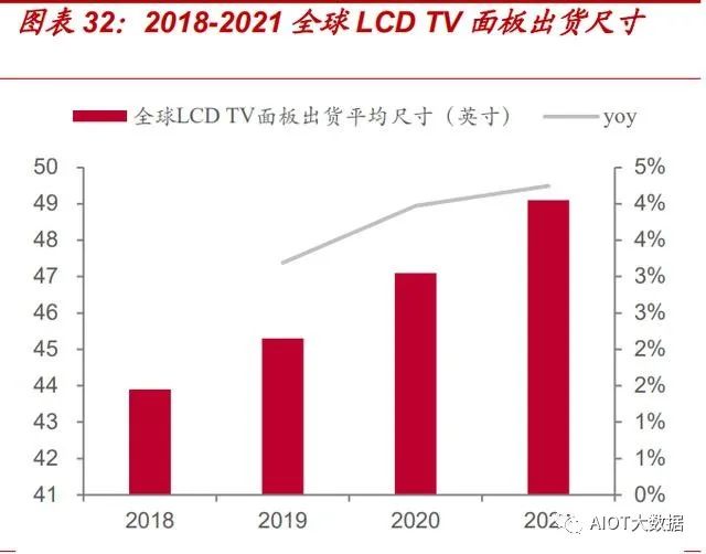
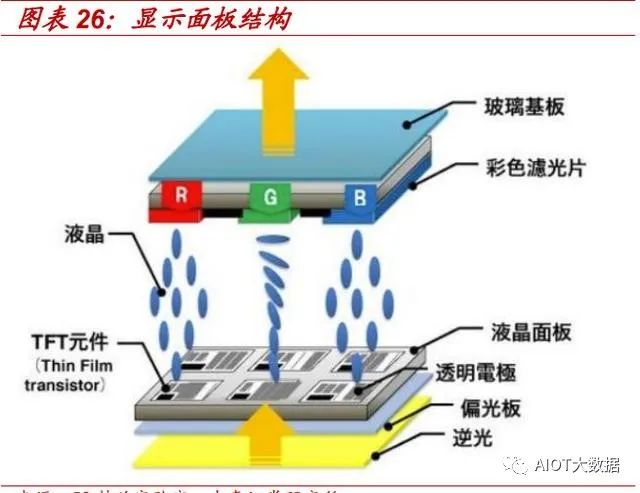 Photoresist accounts for about 10% of the manufacturing cost of LCD panels, directly benefiting from the expansion of the LCD market. According to TrendBank data, color filters account for 21% of panel costs. Color photoresists and black photoresists are core materials for preparing color filters, accounting for about 46% of the overall cost of color filter materials. Thus, it can be estimated that photoresist accounts for approximately 9.66% of the cost of LCD panels, and the market for photoresists directly benefits from the expansion of the LCD market.The global LCD photoresist market size exceeds 1.3 billion USD, with a CAGR of 2% from 2021 to 2026. According to QY research, the global LCD photoresist market is steadily rising, reaching 1.398 billion USD in 2020, and is expected to reach 1.575 billion USD by 2026. The CAGR from 2020 to 2026 is 2%. In the future, it is expected to benefit from the trend of larger sizes and higher definitions of LCD TVs, with the area of LCD panel shipments continuously increasing, which will fully transmit to the demand for panel photoresists. According to Zhiyan Consulting data, it is expected that from 2019 to 2023, China’s LCD photoresist market size will increase from 4 billion RMB to 6.9 billion RMB, with a 4-year CAGR of 14.6%, and the domestic market share is also expected to increase from 47.9% in 2019 to 74.6% in 2023.The global shipment size of LCD TV panels continues to grow. According to Qunzhi Consulting data, in 2021, the shipment proportions of 32″ and 43″ panels significantly narrowed, while the shipment proportions of 65″ and 75″ panels increased by 2.8% and 1.2%, respectively, driving an average size increase of 2.0 inches in 2021. The structural differentiation of panel product sizes has emerged; on the one hand, the pandemic has weakened the purchasing power of consumers in emerging countries, significantly impacting the demand for small and medium-sized TVs, while consumers in developed economies have maintained relatively strong purchasing power, driving strong demand for larger sizes. On the other hand, driven by the rapid rise in overall machine costs, brands are accelerating product structure upgrades to reduce small sizes and increase the proportion of large-size products. Driven by the demand side’s size structure, panel manufacturers are also actively promoting product structure optimization, continuously increasing the capacity proportion of large sizes while controlling the output of small sizes.According to data from the China Business Industry Research Institute, in 2014, the global TFT-LCD display panel shipment area was 166 million square meters, increasing to 223 million square meters in 2019, with an average annual compound growth rate of about 6.07%. As the 5G technology gradually matures and is applied, the trend of large sizes in TFT-LCD panels can better meet the demands of high-definition applications, thus driving the continuous growth of TFT-LCD panel demand. From 2019 to 2023, the shipment area of TFT-LCD panels is expected to increase from 223 million square meters to 249 million square meters, with an increase of 12.20%.
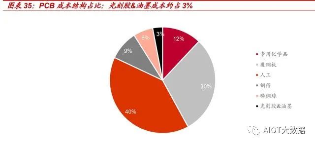
 The continuous transfer of the industry provides a huge market for domestic LCD photoresists. As Japan, South Korea, and Taiwan slow down the construction of new LCD production lines or even shut down existing lines, and as manufacturers in mainland China rise, the construction of panel production lines in mainland China is active, providing a major market for new display devices and raw materials worldwide.The four major domestic manufacturers have occupied more than half of the LCD panel industry’s shipment area. According to Qunzhi Consulting data, in the first half of 2021, BOE, TCL Huaxing, Huike, and Rainbow Optoelectronics had shipment areas of 20.5, 14.9, 8.5, and 5 million square meters, respectively, accounting for 58.1% of the shipment area of the top ten panel manufacturers globally. It is expected that as the industry transfer continues and the production capacity under construction is released, the combined shipment area of domestic manufacturers will reach about 67% by 2023.2.3 PCB Photoresists: Industrial Transfer is the Main Driving ForcePhotoresists are used in PCB processing and manufacturing for pattern transfer. The processing and manufacturing process of PCBs involves pattern transfer, which is to transfer the completed circuit image onto the substrate, thus utilizing photoresists in this process. The basic process is as follows: first, a layer of photoresist film is formed on the substrate surface, and then ultraviolet light is passed through a mask to irradiate the photoresist film. The exposed areas undergo a series of chemical reactions, and then through development, the exposed areas (positive) or unexposed areas (negative) are dissolved and removed, followed by a series of processes such as curing, etching, and stripping to transfer the pattern onto the substrate.PCB photoresists specifically include dry film photoresists, wet film photoresists (also known as etchants/circuit inks), and photo imaging solder masks, which are important upstream materials in the PCB industry, accounting for about 3% of PCB cost structure.
 As the PCB industry transfers to China, China’s PCB photoresist industry has also developed accordingly. Before 1990, the global PCB market was dominated by Europe, America, and Japan, and at that time, China’s PCB photoresist products relied on imports. Since the mid-1990s, the PCB industry began to transfer, and from 2002, foreign-funded PCB photoresist companies began to establish factories in China. By 2017, China’s PCB output accounted for 50.8% of the global total, and the output of PCB photoresists exceeded 70% globally, reaching a market share of 93.35% by 2019, mainly concentrated in the mid-to-low-end product market.The global PCB output has steadily increased, benefiting photoresists. Affected by the pandemic in 2020, the global economy shrank overall, while the PCB market rebounded strongly, achieving a growth rate of 6.4%, mainly driven by the growth in demand for packaging substrates, HDI, and high multilayer boards. According to Prismark’s Q4 2020 report, in the medium to long term, the PCB industry is expected to maintain a stable growth trend, with a projected CAGR of about 5.8% for global PCB output from 2020 to 2025.Regionally, according to Prismark’s forecast, the PCB industry in various regions is expected to show relatively rapid development. In 2020, the predicted year-on-year growth in China is 6.4%, with a compound growth rate of 5.6% from 2020 to 2025. Japan and Asia (mainly Taiwan and South Korea) are the main suppliers of global packaging substrates, and are expected to show high growth rates over the next five years.
3 Oligopoly by the US and Japan, Urgent Need for Domestic Substitution
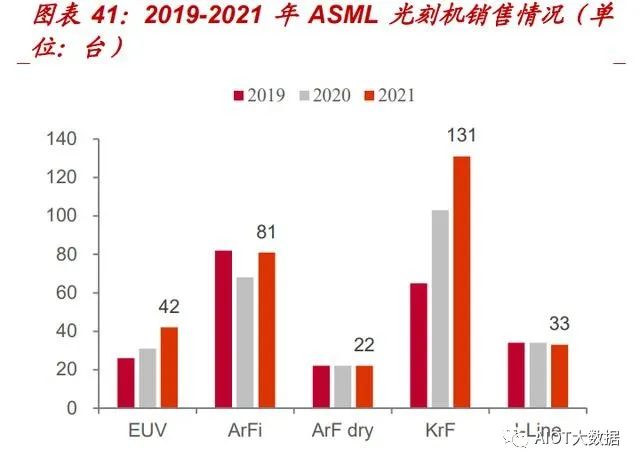
3.1 Four Major Barriers Create High Concentration, Global Market Oligopoly by the US and JapanThe production process of photoresist is complex, and four major barriers create high entry thresholds.The first barrier: technical barriers, high production process requirements, and formulation is fundamental.As the core of the photolithography process, photoresist must meet four major conditions. The factors determining the choice of photoresist are the size requirements of the wafer surface. Photoresist must simultaneously meet the following four conditions: 1) Produce the required size. 2) During the etching process, it must have the function of blocking etching, and there must be no pinholes in the photoresist layer of a specific thickness. 3) It must adhere well to the surface of the wafer (or other substrates), otherwise the etched pattern may become distorted. 4) Process dimensions and step coverage capability.Multiple parameter requirements directly determine product feature sizes. The main performance indicators of photoresist include: resolution, adhesion, contrast, sensitivity, etch resistance, surface tension, exposure speed, pinhole density, and step coverage. 1) Resolution: The smallest pattern or spacing that can be produced in the photoresist layer. Generally speaking, smaller line widths require thinner photoresist films, but to block etching and avoid pinholes, the photoresist film must have a certain thickness, so a trade-off must be made. 2) Adhesion: The photoresist must adhere well to the substrate surface to accurately transfer the pattern to the substrate surface, otherwise it may lead to pattern distortion. During manufacturing, the adhesion of photoresist varies with different surfaces. Therefore, multiple steps in the photoresist process are designed to enhance the natural adhesion of the photoresist to the wafer surface. 3) Exposure speed: The faster the reaction speed, the faster the processing speed in lithography and etching areas. Generally, negative resists require 5-15 seconds of exposure time, while positive resists require 3-4 times longer. 4) Pinhole: Very small holes in the photoresist layer. The presence of pinholes allows etchants to penetrate through the photoresist layer and contact the substrate surface, thereby etching small holes on the substrate surface, causing damage. The thinner the photoresist, the more pinholes there are; the thicker the photoresist, the fewer pinholes there are, but thicker resists reduce the resolution of the photoresist, so the thickness of the photoresist film is a trade-off of multiple factors.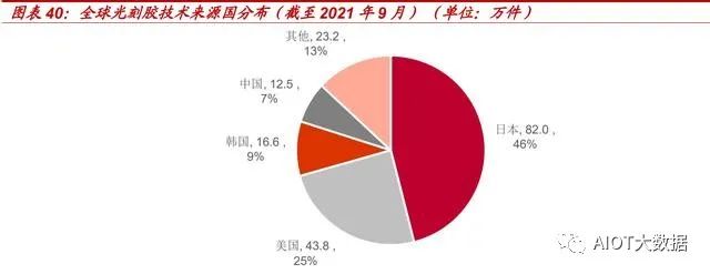 Once the photoresist process is established, it generally will not change. The preparation, baking, exposure, etching, and removal processes will be fine-tuned according to the specific properties of the photoresist and the expected results. The selection of photoresist and the development of photoresist processes is a long and complex process, and once a photolithography process is established, it is generally not changed.In terms of the number of patents, Japan and the US account for over 70%, with rapid development in mainland China. According to Zhihuiya data, as of September 2021, Japan is the largest source country for photoresist technology, accounting for 46% of global photoresist patent applications; the US ranks second with 25%. China ranks behind South Korea with a 7% application rate. From a trend perspective, the number of photoresist-related patent applications in China is rapidly increasing, surpassing Japan in 2020. In 2020, the number of photoresist patent applications in China reached 12,900, while Japan’s declined to 8,982.Photoresists come in various types, with different chemical structures and performance characteristics. There are significant differences in the needs of downstream customers for different types of photoresist, even for the same customer’s different application needs. This leads to a lack of unified processes in the overall production of photoresist, as the raw materials used for each type of photoresist differ in chemical structure and performance, requiring the use of different grades of specialized chemicals. This forces manufacturers to have the capability to design different formulations to meet diverse needs and to have corresponding production processes to complete production. This is one of the core technologies of the industry, requiring high technical capabilities from enterprises.The second barrier: customer certification barriers, deeply binding upstream and downstream, with long verification cycles.Before supplying photoresist, it generally undergoes verification of the product and the qualification of the factory (production line). The verification of photoresist is divided into PRS (photoresist performance testing), STR (small-scale testing), MSTR (batch verification), and Release (passing verification); the qualification of the factory (production line) involves verification of quality systems, supply stability, production capacity, etc. After the factory (production line) qualification is passed and the product is verified, formal supply to customers can be realized. Due to the verification cycle usually being 6-24 months, the cost of switching photoresist for downstream foundries is high, and customers are generally unwilling to switch photoresist, making it difficult for photoresist companies to break through customer barriers.The third barrier: equipment barriers, expensive photolithography machines that are difficult to purchase.Before sample submission, photoresist manufacturers need to purchase photolithography machines for internal formulation testing and adjust formulations based on verification results. Photolithography equipment is expensive, limited in number, and its supply may be restricted by foreign countries, especially since currently only ASML can supply EUV photolithography machines in bulk.The delivery cycle for purchasing photolithography machines is long. According to Nikkei Asia Review reports, due to demand exceeding capacity, the delivery time for chip production equipment has increased from 12 months to about 18 months.With low production and high prices, recent increases have mainly focused on EUV, ArFi, and KrF photolithography machines. According to ASML’s 2021 financial report, the company sold a total of 287 photolithography systems in 2021, with sales of approximately 13.65 billion euros, of which 42 were EUV photolithography systems with sales of about 6.28 billion euros, averaging 150 million euros each; 81 ArFi photolithography systems with sales of about 4.96 billion euros, averaging about 61 million euros each; 22 ArF dry photolithography systems with sales of about 430 million euros, averaging about 20 million euros each; and 131 KrF photolithography systems with sales of approximately 1.32 billion euros, averaging about 10 million euros each; and 33 i-line photolithography systems with sales of about 140 million euros, averaging about 4 million euros each.
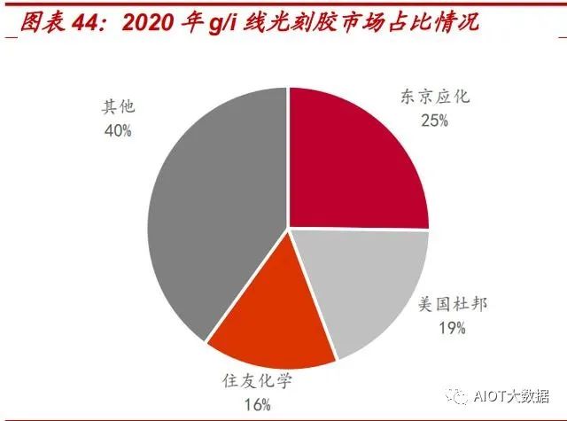
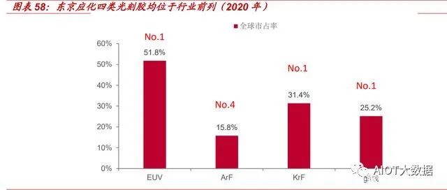
 The fourth barrier: raw material barriers, as the domestic industrial chain is not yet complete, with many difficulties in the industrialization of resins and monomers.Upstream raw materials are important factors affecting the quality of photoresist. Currently, the market for raw materials for photoresist in China is basically monopolized by foreign manufacturers, especially resins and photosensitizers, which are highly dependent on imports, resulting in a low domestic substitution rate, thereby increasing the production costs and supply chain risks of domestic photoresists.The industry is highly concentrated, with Japanese and American companies monopolizing the market. The global photoresist market is basically monopolized by Japanese and American companies. Data from 2020 shows that Tokyo Ohka ranked first with a share of 26%, DuPont ranked second with a share of 17%, along with JSR and Sumitomo Chemical, with CR4 close to 70%, indicating a high concentration in the industry.From the perspective of semiconductor photoresist sub-products, major giants focus more on mid-to-high-end photoresists. Currently, Tokyo Ohka ranks first in overall strength, and although it ranks fourth in the ArF photoresist field with a market share of 16%, it ranks first in the other three fields, dominating the EUV photoresist field with more than half of the share.PCB photoresists: Domestic companies dominate low-end products. In the PCB photoresist market, China occupies a leading position in mid-to-low-end products, with domestic companies like Ronda, Guangxin Materials, Dongfang Materials, and Beijing Litod occupying about 46% of the domestic wet film photoresist and photo imaging solder mask market. However, the high-end dry film photoresist market is mainly monopolized by Japan’s Asahi Kasei, Japan’s Hitachi Chemical, and Taiwan’s Changchun Chemical, with these three companies holding over 80% of the global market share, while China still relies heavily on imports for dry film photoresists.
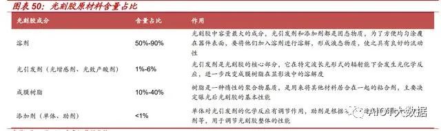
 The global supply of LCD photoresists is concentrated in Japan, South Korea, and Taiwan, with the domestic color and black photoresist market having a domestic substitution rate of only about 5%. The high molecular pigments and dispersion technologies required for color filters are mainly concentrated in Japanese pigment manufacturers such as Ciba, so the core technologies for color and black photoresists are basically monopolized by Japanese and Korean companies. On the other hand, in recent years, China has made breakthroughs in touch screen photoresist technology, with companies like Crystal Ray and Beijing Kehua Micro already achieving mass production of touch screen photoresists, with a domestic substitution rate of about 30%-40%.3.2 The Upstream Raw Materials of Resins and Monomers Are Difficult, and the Mainland’s Industrialization Is Awaiting BreakthroughsSolvents, photosensitizers, and resins are the three main raw materials for photoresists. Photoresists are adjusted based on different wavelengths of light and exposure sources. Photoresists have specific thermal flow characteristics and are formulated using specific methods to bond with specific surfaces. These properties are determined by the types, quantities, and mixing processes of different chemical components in the photoresist, with solvents accounting for 50%-90%, resins for 10%-40%, photosensitizers for 1%-6%, and additives for less than 1% of the total composition. Solvents are the largest component in photoresists, keeping them in liquid form and allowing them to be spun onto the surface of the wafer to form a thin layer. Photosensitizers control or adjust the chemical reactions of the photoresist during exposure, used to generate or control specific reactions of the polymer. Photosensitizers are added to photoresists to limit the spectral range of the exposure light or restrict the reaction light to specific wavelengths. Polymers are used to change from soluble to aggregate (or vice versa) when exposed to light, consisting of large, heavy molecules that include carbon, hydrogen, and oxygen, with typical polymers being plastics. Additionally, photoresists contain additives. Different types of additives are mixed into the photoresist to achieve specific results. Some negative resists contain dyes that serve to absorb and control light within the photoresist film. Positive resists may contain chemical anti-dissolution systems, which can prevent unexposed parts of the photoresist from dissolving during the development process.In terms of cost, in high-end photoresists, resins account for a large proportion of costs. According to Nanda Optoelectronics’ announcements, ArF photoresist resins mainly consist of propylene glycol methyl ether acetate, which accounts for only 5%-10% of the total weight, but over 97% of the total cost of raw materials for photoresists.
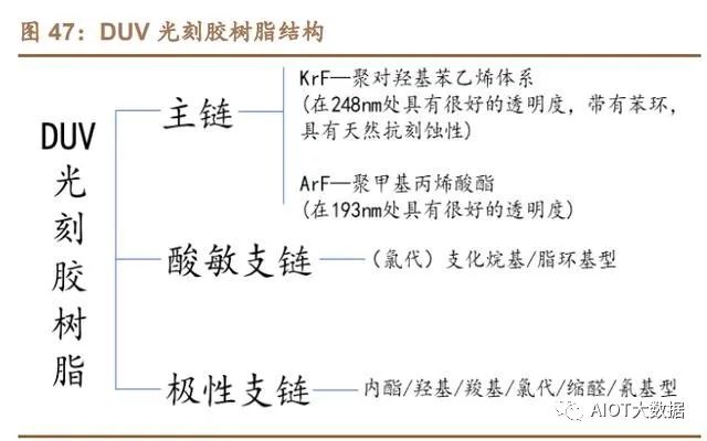
 1) Resins: Overseas monopolize the market, while mainland enterprises have made technological breakthroughs.Most of the resins needed for various types of photoresists are monopolized by overseas manufacturers. G-line photoresists use cyclized rubber resins; I-line photoresists use linear phenolic resins, which mainly rely on imports, and the level of domestic substitution is very low. For domestic photoresists that are “choked” by KrF and ArF photoresists, KrF uses polyhydroxy styrene resins, which are basically imported. This is because the monomers needed to produce resins are rarely supplied by domestic manufacturers, and the production processes for resins also have certain difficulties, especially in post-processing. ArF uses polymethyl methacrylate resins, with monomers derived from methacrylic acid and acrylate derivatives, and ArF resins are formed by copolymerization of several monomers, requiring a high degree of customization, making high-end ArF resins almost impossible to purchase. EUV uses polyhydroxy styrene resins or molecular glasses and metal oxides, with almost no domestic production.There are currently two major categories of global photoresist resin manufacturers. One type is photoresist manufacturers that produce their own resins, such as Shin-Etsu Chemical and DuPont, which usually hold patents for resin synthesis and photoresist formulation technology. The other type consists of specialized resin manufacturers, such as Toyo Gosei, Sumitomo Bakelite, and Mitsubishi Chemical, which provide customized resins for photoresist manufacturers.The high technical barriers remain the fundamental reason for overseas monopolization. The structural design of resins involves the types and ratios of monomers, which determine the line widths (CD), exposure energy (EOP), energy window (EL), and line width roughness (LWR) that photoresists can achieve at specific wavelengths. In addition, the molecular weight, PDI (polydispersity index), etc., of the resins can also affect the thickness, etch resistance, and adhesion of the photoresist films. Resins can be synthesized through various methods: photoresist resins can be synthesized through phenolic condensation reactions, cationic polymerization, anionic polymerization, and active radical polymerization methods. The upstream raw materials are mainly monomers, which polymerize into resins during the polymer synthesis process.The major difficulties of resin synthesis are: 1) achieving consistent quality, with molecular weight and molecular weight distribution being very close for each batch; 2) higher-grade resins have smaller molecular weight distributions; 3) metal ion requirements, most of which require less than 1ppb, and even to ppt level.The five major challenges of industrialization include: 1) Synthesis technology: Resin synthesis technology can be divided into radical polymerization, anionic polymerization, and active radical polymerization. Currently, the most commonly used is radical polymerization, while active radical polymerization has not yet achieved industrialization. 2) Stability in scaling up and removal of metal ions: Scaling up refers to the evolution of resin from laboratory research to industrial-scale production, and stability in scaling up mainly refers to the consistency of molecular weight and PDI for each production run, requiring strict management and quality control. 3) Stable supply: The supply of monomers must be stable, and the quality of monomers must also be stable. For downstream customers, resins must also achieve stable supply, including stable quality and delivery cycles. 4) Customer certification and procurement: Customer certification and procurement is a long-term process. After a photoresist manufacturer formulates a resin from a supplier, it must send samples to downstream foundries for testing to determine whether the resin’s lithographic performance is good and whether to adopt that supplier’s resin. Additionally, photoresist manufacturers must notify downstream foundries when changing resin suppliers. 5) Scale effects: Photoresist resins are generally customized products. Without commercialized resins or other products to support, solely producing a certain type or category of photoresist resin will lead companies to lose motivation for R&D or production of photoresist resins, especially when monomers need to be purchased, as high costs will greatly affect the profitability of the resins.
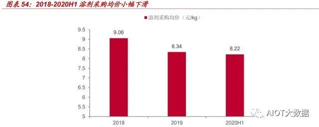
 2) Monomers: Japanese and American companies dominate the market.Different types of photoresists have corresponding photoresist monomers. Traditional I-line monomers are mainly methyl phenol and formaldehyde, which are bulk chemicals; KrF monomers are mainly styrene-based monomers, which are liquid; ArF monomers are mainly methacrylate-based monomers, which can be either solid or liquid. The performance indicators of photoresist monomers include purity, moisture, acidity, single impurities, and metal ion content.Semiconductor-grade photoresist monomers have a higher barrier than ordinary monomers. 1) The synthesis technology of semiconductor-grade photoresist monomers is more difficult. 2) Semiconductor-grade photoresist monomers require more stable quality, with fewer metal ion impurities. For example, semiconductor-grade monomers require a purity of 99.5%, with metal ion content less than 1ppb (i.e., one part per billion); while panel-grade monomers are epoxy-based, with purity requirements of only 99.0%, and metal ion content of less than 100ppb is acceptable. 3) The prices of semiconductor-grade photoresist monomers are much higher than those of ordinary monomers. I-line monomers are about 100-200 RMB/kg, KrF monomers are about 500-1000 RMB/kg, while ArF dry and wet monomers range from 3000-10000 RMB/kg.There are six major difficulties in industrialization: 1) During synthesis and purification, it is necessary to prevent monomer polymerization; 2) There are many types of photoresist monomers, and different synthesis methods must be studied for different monomers, with varying degrees of difficulty. 3) High purity requirements: High purity must be defined from different indicators, such as gas phase (GC), liquid phase (HPLC), gel permeation chromatography (GPC), etc., and sometimes purity must reach over 99.9%. 4) Control of metal ions: The metal ion content in semiconductor-grade monomers, especially in ArF monomers, must be less than 1ppb. 5) Process scaling: Monomers that meet standards produced in laboratories may not meet customer needs, and stable large-scale production is required for industrial-grade supply. 6) Photoresist monomer companies need a long certification process to enter the downstream customer’s supply system, and they generally will not easily change.3) Solvents: Currently, the main solvent for photoresists is PGMEA (propylene glycol methyl ether acetate), with a high self-sufficiency rate in the mainland. According to data from the New Thinking Industry Research Center, China is the world’s largest PGMEA producer, accounting for about 35% of global total production, with companies such as Baichuan Co., Ruijia Chemical, Yida Chemical, Warren, and Denka International among the producers. In the global market, PGMEA production is dominated by companies such as Dow Chemical, Shell Chemicals, LyondellBasell Industries, and Eastman Chemical, which together account for more than half of the global market share.According to Ronda’s announcements, the average procurement price of solvents in the first half of 2020 was 8.22 RMB/kg, which has decreased compared to 2018 and 2019. (Report source: Future Think Tank)
 4) Photoinitiators: Concentration trends are becoming increasingly apparent, and historical procurement prices are on a downward trend.Photoinitiators are the core raw materials for photopolymerization materials (mainly including UV coatings, UV inks, UV adhesives, etc.). Photopolymerization materials are important alternatives to traditional solvent-based coatings, inks, and adhesives. In 2020, the global photoinitiator market sales reached 680 million USD, and it is expected to reach approximately 1.1 billion USD by 2027, with a CAGR of 4.57% from 2020 to 2027.The main companies in the photoinitiator field include IGM Resins, Tianjin Jiuri New Materials, Changzhou Qiangli, and Arkema; among them, IGM Resins is the global market leader, accounting for 27% of the global market share in 2020. Tianjin Jiuri New Materials is the domestic market leader, accounting for 28% of the Chinese market share in 2020. The UV coating manufacturing industry is the largest demand sector for photoinitiators, requiring suppliers to provide reliable quality, cost-effective products, and stable supply. As downstream customer requirements are high, the concentration of the industry is increasing. From the perspective of procurement prices of photoinitiators, according to data disclosed by Ronda, from 2018 to the first half of 2020, as the competitive structure of upstream suppliers gradually stabilizes, the procurement prices of photoinitiators have generally declined, with the average procurement price in the first half of 2020 being 131.46 RMB/kg, indicating a historical downward trend in procurement prices.3.3 Japanese Industry Leaders Have Strong Strength, and Domestic Manufacturers Hope to Replicate Successful ExperiencesThe photoresist industry was initially dominated by Europe and the United States, with Japanese manufacturers later catching up. In 1839, the first “photoresist system” made of dichromate gelatin was born. After a century of development, photoresist technology began to mature. In the 1950s, Germany’s Kalle company produced diazo naphthoquinone-phenolic resin printing materials, and the exposure light sources could be g-line or i-line. In the 1980s, IBM used self-developed KrF photoresists to break through KrF lithography technology. Subsequently, Tokyo Ohka developed KrF positive photoresists in 1995 and achieved large-scale commercialization, quickly dominating the market, marking the official entry of Japanese manufacturers into the dominant era of photoresists.JSR: The leading photoresist manufacturer originating from synthetic resins. The company started with latex business, and since synthetic resins are also one of the main materials for photoresists, JSR began to enter the photoresist field in the early 1980s through resin technology. Over the past 40 years, JSR’s photoresist business has progressed with semiconductor process technology, and the company’s semiconductor photoresists now cover the entire range from g-line to EUV photoresists.From immersion ArF photoresists to EUV extreme ultraviolet photoresists, JSR has played a pioneering role in every technological transformation of photoresists. JSR is mainly divided into two business divisions: petrochemical and fine chemicals, with the fine chemicals division including semiconductor materials, display materials, and edge computing materials; JSR’s conductor materials include photoresists, CMP materials, packaging testing materials, and display materials include LCD panel materials, reflective film materials, and other functional coating materials.TOK: Dominating the EUV photoresist market. TOK is a long-established Japanese chemical materials company. The company was founded in 1940, and in 1968 and 1972, it developed positive and negative photoresists for semiconductors, aiming to become a leading supplier of photoresists and staying at the forefront of semiconductor micro-processing technology. As early as 2006, Tokyo Ohka began to invest in the research and development of the technologies required for ArF immersion photoresists and has maintained a leading position in the global photoresist market.Tokyo Ohka has a complete layout in semiconductor photoresists. In 2020, it held market shares of 25.2%, 31.4%, 15.8%, and 51.8% in g/i photoresists, KrF, ArF, and EUV photoresists, respectively, making it an undisputed leader in the global photoresist industry.
 The technical level and production quality are industry-leading, with a complete customer layout in China: Tokyo Ohka focuses more on the application of photoresist materials and their auxiliary materials in various scenarios. Its photoresist products are at the forefront of the industry in terms of both technical level and production quality. Tokyo Ohka has over 10 years of operational history in China, with representative manufacturers such as TSMC, SMIC, Huahong NEC, Hongli, and Hejian as its customers in the region.Shin-Etsu Chemical: A comprehensive semiconductor materials leader. Shin-Etsu Chemical was founded in 1926, initially focusing on nitrogen fertilizers, and expanded into semiconductor materials with the support of the Japanese government after World War II. After more than half a century of development, Shin-Etsu Chemical has successfully established a global production and sales network for self-developed materials such as polyvinyl chloride, organosilicon, and cellulose derivatives in countries and regions including the United States, Japan, the Netherlands, South Korea, Singapore, and China.In the semiconductor materials field, Shin-Etsu Chemical has gradually overcome technical challenges in high-purity hydrofluoric acid, high-purity single crystal silicon, rare earth magnets, photoresists, LED packaging, and power semiconductor materials.
4 Extremely Low Domestic Substitution Rate Combined with Overseas Supply Disruptions, Urgent Need for Mainland Industrial Chain to Rise
The domestic substitution rate of photoresists in mainland China is extremely low. Semiconductor photoresists are monopolized by Japanese companies, with a domestic substitution rate of only 10%. Currently, China has only achieved mass production of g-line, i-line, and KrF photoresists, while ArF photoresists are mostly in the research and sample submission stage, and EUV photoresists are still in the early research stage. For flat panel display photoresists, the main production areas are Japan, South Korea, and Taiwan, with the domestic color photoresists and black photoresists having a domestic substitution rate of only about 5%. After acquiring LG Chem’s business in this sector, Yake Technology has become the largest domestic supplier. For TFT photoresists, most of the production capacity in mainland China is still imported.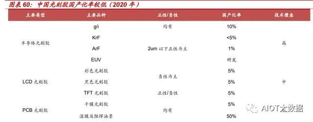 The mainland enterprises have layouts in upstream raw materials. From the perspective of A-share listed companies’ layouts in photoresist raw materials, solvent companies include Baichuan Co. and Yida Co.; monomer companies include Huamao Technology (investing in Xuzhou BOKANG), and Lianrui New Materials; resin companies include Tongcheng New Materials, Shengquan Group, and Qiangli New Materials; photoinitiator companies include Qiangli New Materials.In terms of midstream manufacturing, domestic companies have made milestone breakthroughs in g/i line photoresists, continuously striving for mid-to-high-end KrF and ArF photoresists. Currently, domestic photoresists have achieved significant breakthroughs in midstream manufacturing, with a number of excellent companies emerging. In the semiconductor photoresist field, Tongcheng New Materials (which supplies KrF photoresists in bulk to SMIC and Changchun) has a market share of 60% for g-line photoresists; Jingrui Electromaterials (which has supplied g/i line photoresists for years and has tested KrF) is making progress; Shanghai XinYang (which has formed sales for KrF and is progressing well in ArF research); Huamao Technology (investing in Xuzhou BOKANG, with full industrial chain capabilities for photoresists). In 2022, domestic semiconductor photoresists are expected to flourish and achieve volume production.4.2 Tongcheng New Materials: Domestic Leader in KrF Photoresists with Integrated Industrial AdvantagesTongcheng New Materials is a global leading new materials comprehensive service provider, with main businesses including electronic materials, automotive materials, and biodegradable materials. In the photoresist field, the company invested in and controlled “Kehua + Beixu” to enter the track, where Beijing Kehua is a leading domestic semiconductor photoresist manufacturer and is listed among the global top eight photoresist companies by SEMI, and is also the only company in China to achieve batch production of KrF photoresists. Beixu Electronics is a pioneer in the domestic LCD photoresist market, specializing in organic positive photoresists and inorganic special powders.In 2021, the company’s revenue reached 2.308 billion RMB, an increase of 12.83% year-on-year, with photoresist business revenue reaching 115 million RMB, a year-on-year growth of 28.8%. The company possesses advantages in technology, scale, and integrated industrial chain, and is expected to experience rapid growth with the release of mature products and breakthroughs in new product research and development. In the KrF photoresist field, the company is the first domestic supplier, having become a partner of major clients such as SMIC, Shanghai Huahong Microelectronics, Changjiang Storage, Wuhan Xinxin, and Huahong Semiconductor. In the ArF photoresist field, the company has self-raised 698 million RMB to invest in the construction of an “ArF High-end Photoresist R&D Platform Project,” aiming for mass production of ArF wet photoresists, with the project expected to be completed by the end of 2023.4.3 Huamao Technology: Domestic Giant in Photoresist Monomers with Strong Upstream and Downstream Integration CapabilitiesHuamao Technology is a leading enterprise in the domestic automotive passive safety industry. In 2020, the company invested in Xuzhou Kangbo to enter the semiconductor photoresist field, creating a second growth driver. With the recovery of the downstream automotive market and the release of new semiconductor material products, the company has made significant progress. In 2021, it achieved revenue of 1.206 billion RMB, a year-on-year increase of 27.01%; excluding the impact of share payments, the net profit reached 228 million RMB, a year-on-year increase of 16.84%.The company has excellent upstream and downstream integration capabilities. In the upstream raw material field, its subsidiary Xuzhou BOKANG is a leading domestic photoresist monomer supplier, with all its photoresist monomer products achieving self-supply; in the photolithography machine field, its subsidiary UK NBL has the capability to develop and produce high-end electron beam photolithography machines. In the KrF photoresist field, in April 2022, its subsidiary Xuzhou BOKANG received orders from mainstream memory chip manufacturers in mainland China, marking the product’s formal recognition by mainstream 12-inch wafer manufacturers in mainland China. In the ArF photoresist field, the company has the technical capabilities for both dry and wet ArF photoresists.4.4 Nanda Optoelectronics: A Pioneer in Domestic ArF Photoresists, Advancing Multiple Business Lines SimultaneouslyNanda Optoelectronics is one of the major suppliers of MO sources globally. Backed by Nanda’s technical background, the company strategically lays out three key semiconductor materials. With significant breakthroughs in major technological projects, the company’s core growth and business synergy effects are gradually becoming apparent, greatly enhancing its market and brand image, and achieving rapid growth in performance. In 2021, the company achieved revenue of 984 million RMB, a year-on-year increase of 65.46%; its net profit reached 136 million RMB, a year-on-year increase of 56.55%.In the ArF photoresist field, in December 2020, the company’s ArF photoresist products passed certification on a 50nm flash memory platform at a storage chip manufacturing company, and in May 2021, it achieved certification breakthroughs on products at a 55nm technology node for logic chip manufacturers. Meanwhile, Nanda Optoelectronics is constructing a production line for ArF photoresists with an annual capacity of 25 tons, and has initially realized the localization of raw materials. In the future, with smooth downstream customer introduction and production line launch, the company is expected to become a leader and breakthrough player in domestic ArF photoresists.4.5 Jingrui Electromaterials: A Pioneer in Domestic Photoresists, Actively Building KrF Mass Production LinesJingrui Electromaterials is a technology-based new materials company, and its subsidiary Suzhou Ruihong has been a pioneer in the domestic photoresist field, producing photoresists for nearly 30 years, primarily applied in the semiconductor and flat panel display fields, with its product technology level and sales volume leading domestically. With steady increases in the company’s capacity and simultaneous rises in both volume and price of its main products, the company has seen remarkable growth, achieving revenue of 1.832 billion RMB in 2021, a year-on-year increase of 79.2%, with photoresists and supporting materials achieving revenue of 274 million RMB, a year-on-year increase of 53.1%; its net profit reached 201 million RMB, a year-on-year increase of 161.2%.In the i-line photoresist field, the company undertook and completed the national major science and technology project 02, “Development and Industrialization of i-Line Photoresists,” and its products have been supplied to well-known large-size semiconductor manufacturers such as SMIC and Changxin. In the KrF photoresist field, as of August 2021, the company has completed pilot testing and established a pilot demonstration line, entering the customer testing phase. In December 2021, the company purchased a KrF photolithography machine for exposure testing, and related mass production lines are actively being constructed. Currently, the company is building a key electronic materials project in Meishan with an annual output of 1,200 tons, with a planned capacity of 1,000 tons/year for intermediates and 1,200 tons/year for photoresists, with an expected construction period of one year.Source: AIOT Big Data (Report produced by Zhongtai Securities, Wang Fang, Yang Xu)