The comprehensive analysis series of semiconductors consists of three articles, this one is the market analysis, and the next two will be technical and industrial analyses. Please follow this public account (Shichenxing shichenxing1) for updates.
1. Two Main Characteristics
1. Energy Band
Conductors are easy to understand, and insulators are also understandable, but the concept of semiconductors might be confusing.
When atoms form a substance, many electrons will mix together, but two identical electrons cannot occupy the same orbital. Thus, many orbitals split into several orbitals. When so many orbitals are crowded together, they may accidentally get close enough to form a wide band. In quantum mechanics, these fine orbitals are called energy levels, while the wide orbitals that result from crowding together are called energy bands.
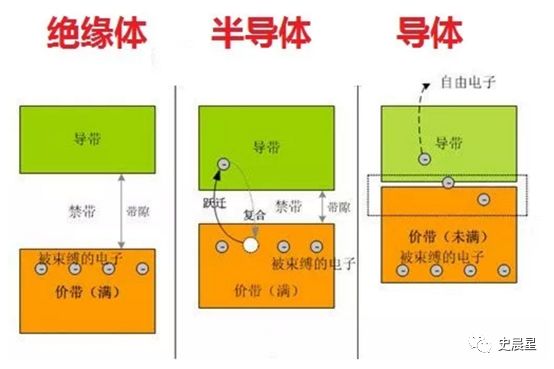
Some wide bands are filled with electrons, and electrons cannot move, which macroscopically manifests as non-conductivity.
Some wide bands have plenty of space, allowing electrons to move freely, which macroscopically manifests as conductivity.
If some filled bands and empty bands are too close, electrons can easily jump from the filled band to the empty band, allowing for free movement; this is what we call a conductor.
If there is a gap between two wide bands, electrons cannot jump across it by themselves, which manifests as non-conductivity.
If the gap width is within 5 eV, providing extra energy to the electrons can allow them to jump to the empty band, enabling free movement and manifesting as conductivity. This type of solid, whose gap width does not exceed 5 eV, can sometimes conduct electricity and sometimes not, hence it is called a semiconductor.
2. Semiconductor
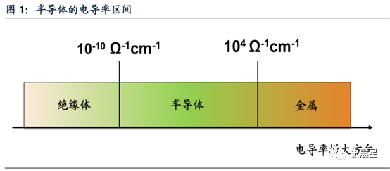
Semiconductor refers to materials that have electrical conductivity between that of a conductor (conductor) and an insulator (insulator) at room temperature.
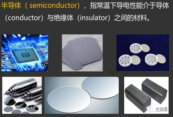
Typically, the electrical conductivity of metals is greater than 10,000 (104) Ω-1cm-1, such as aluminum, copper, silver, platinum, etc., while the electrical conductivity of insulators is less than one billionth (10-10) Ω-1cm-1, such as rubber, ceramics, plastics, etc. A solid material with electrical conductivity between 104 and 10-10 Ω-1cm-1 is referred to as a semiconductor.
Next, let’s engage our brains a bit.
3. Doping Characteristics
The electrical conductivity of semiconductors is not constant; it varies with the doping of impurity elements, temperature, light exposure, external forces, and other external conditions, changing within the range between insulators and metals. These characteristics give semiconductors a rich variety of applications.
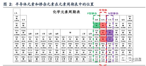
One method is to dope with Group V elements (commonly phosphorus P, arsenic As). Group V elements have one more outer electron compared to Group IV, and this extra electron can serve as a source of conductivity, a doping method known as N (Negative) type doping.
Another method is to dope with Group III elements (commonly boron B, boron fluoride BF2). Group III elements have one less outer electron compared to Group IV, and this missing electron creates a vacancy known as a hole, which can also conduct electricity; this corresponding doping method is called P (Positive) type doping.
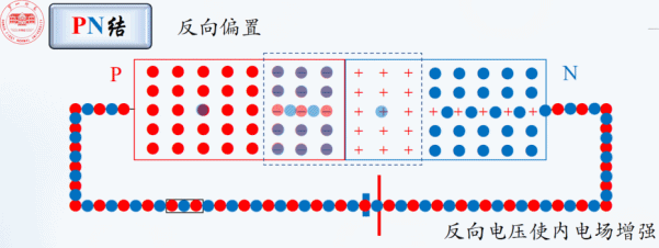
PN Junction
What happens when you place these two types of semiconductors face to face? It’s obvious that the extra electrons from the N-type will inevitably move to fill the vacancies in the P-type until the electric field is balanced, creating the famous PN junction (animated image from Zhang Yun’s blog on Science Net).
The PN junction exhibits unidirectional conductivity, where current can only flow from one side to the other, not the reverse.
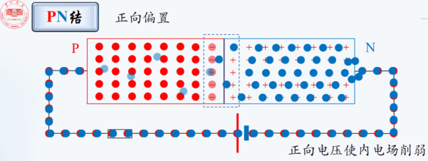
If a forward voltage is applied to the PN junction, with the P region connected to the positive terminal and the N region to the negative terminal, most charge carriers will continuously flow through the PN junction under the influence of the external electric field, forming a large diffusion current, known as forward current.
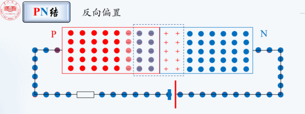
If a reverse voltage is applied, the diffusion movement of most charge carriers weakens, and no forward current flows through the PN junction, only a small drift movement of charge carriers forms a reverse current. Since the minority carriers are very few, the reverse current is weak, resulting in a high resistance.
A single PN junction can form the simplest semiconductor device, a diode, which is also the fundamental structure for constructing other semiconductor devices like transistors (BJT), metal-oxide-semiconductor field-effect transistors (MOSFET), etc.
Let’s look at an example for deeper understanding.
Why does Zhang Wuji have to take off his clothes to transfer internal energy to women, but not to men?
In the context of Zhang Wuji’s transmission of internal energy: assume men are P-type doped and women are N-type doped, with internal energy being the current formed by electron movement, then: when men transfer internal energy to men, the charge carriers move within the same doped semiconductor, which is analogous to moving through a resistor without needing to overcome a barrier.


When men transfer internal energy to women, electrons move through the PN junction and need to overcome the barrier (clothing) to flow, hence the need to reduce the barrier.


4. Photoelectric Characteristics
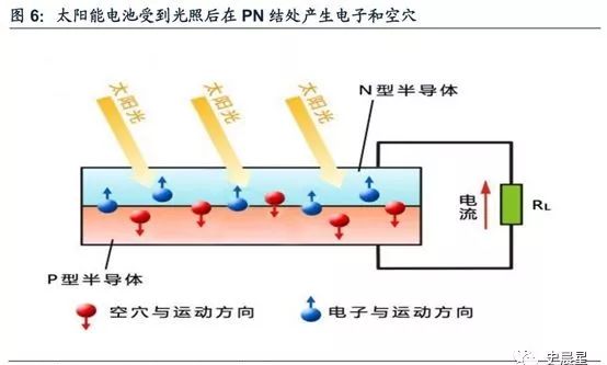
Photogenerated Electricity: At the PN junction, there are no free-moving electrons and holes, but many covalent electrons are bound in the outer layers of lattice atoms. Light can provide energy to these covalent electrons, freeing them from the lattice’s binding and turning them into freely moving electrons and holes. Since both electrons and holes contribute to current, light can generate current at the PN junction. The photogenerated electricity characteristics of the PN junction allow it to be made into avalanche diodes and PIN diodes, which are widely used in photodetectors, solar cells, and other fields.
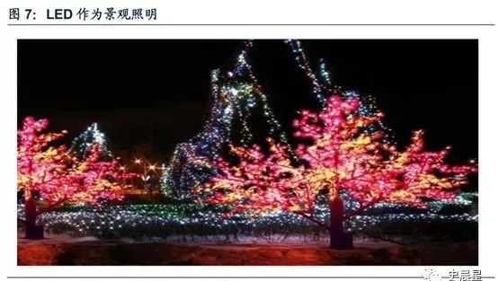
Electroluminescence: Conversely, if a forward voltage is applied across the PN junction, the electrons and holes in the semiconductor will meet at the junction, disappear (recombine), and produce a burst of photons, provided that the material used to create the PN junction is a direct bandgap semiconductor. The electroluminescent characteristics of the PN junction allow it to be made into light-emitting diodes (LEDs), laser diodes (LDs), etc., widely used in semiconductor lighting, optical communication sources, 3D sensing, and other fields.
Direct bandgap semiconductors are materials where the electrons and holes recombine while following momentum conservation, such as compound semiconductor materials: GaAs, GaP, GaN, etc. In contrast, silicon, which is widely used, is an indirect bandgap semiconductor. PN junctions made from silicon can only create diodes with rectifying and switching characteristics and cannot emit photons.
2. Four Major Classifications
5. Four Major Classifications
Semiconductors can be classified into four types of products based on their applications: integrated circuits, optoelectronic devices, discrete devices, and sensors. For detailed analysis, please continue to follow this public account (Shichenxing shichenxing1).
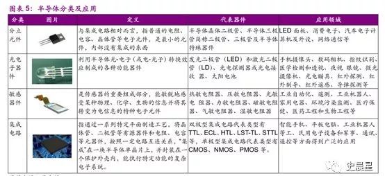
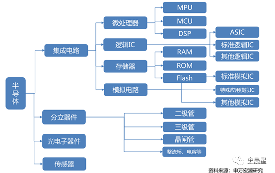
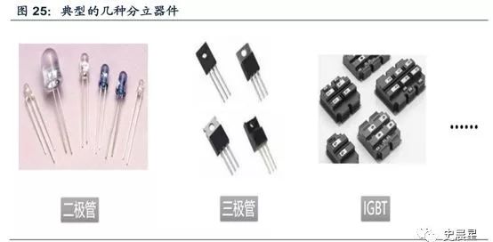
Discrete Devices: Individual diodes, transistors, and power semiconductor devices (such as LDMOS, IGBT, etc.) are classified as discrete devices. Compared to integrated circuits, they are larger in size but have advantages in certain scenarios (such as ultra-high power and semiconductor lighting).
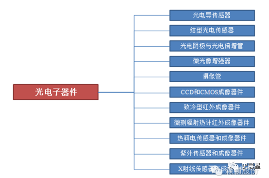
Optoelectronic Devices are various functional devices made using the electro-photon conversion effect. They have a wide range of applications, including optical communication, optical displays, mobile phone cameras, night vision goggles, low-light cameras, photoelectric sights, infrared detection, infrared guidance, medical detection, and imaging.
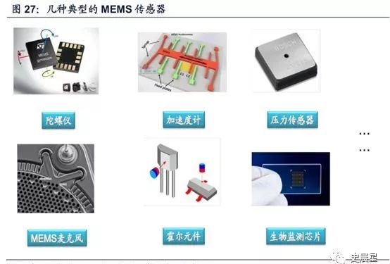
Sensors: Sensors are devices that convert physical quantities in the environment into electrical quantities.
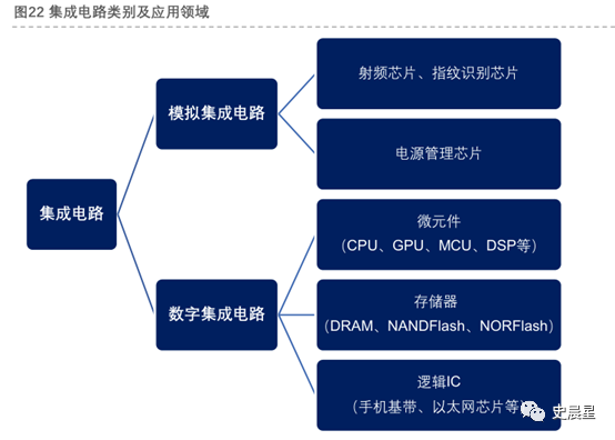
Integrated Circuit (IC) is a type of microelectronic device or component. It uses specific processes to interconnect all required components such as transistors, resistors, capacitors, and inductors on a small piece or several pieces of semiconductor wafers or dielectric substrates, then encapsulates them in a casing to form a microstructure with the desired circuit functions, also known as a chip.

There are many types of chips. Depending on the type of signal processed, they can be classified into analog integrated circuits and digital integrated circuits. For detailed analysis, please continue to follow this public account (Shichenxing shichenxing1).
6. Global Market
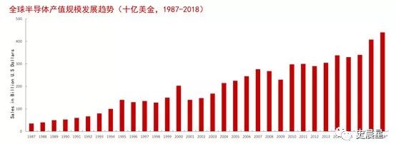
According to the latest data from WSTS, the global semiconductor market reached 478 billion USD in 2018, and it is predicted to reach 490.1 billion USD in 2019.
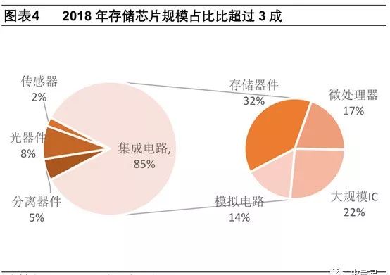
According to WSTS data, the sales of discrete devices amounted to 24.102 billion USD, optoelectronic sales reached 38.032 billion USD, sensor sales were 13.356 billion USD, and integrated circuits (IC) sales reached 393.288 billion USD, accounting for 5.14%, 8.11%, 2.85%, and 83.9% of the global semiconductor sales total, respectively.
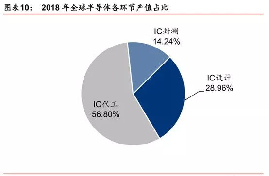
According to IC Insights and Gartner data, the output value of global integrated circuit design was 113.9 billion USD in 2018, the output value of integrated circuit packaging and testing was 56 billion USD, and the output value of IC manufacturing was approximately 223.38 billion USD, with design, manufacturing, and testing accounting for 29%, 57%, and 14% respectively.
7. China
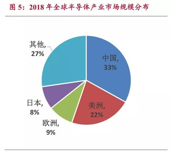
From a market structure perspective, China and the Americas (mainly the USA) have become the top two global semiconductor consumption markets, with their market sizes accounting for 32% and 22% respectively in 2018, followed by Europe and Japan.
8. Applications
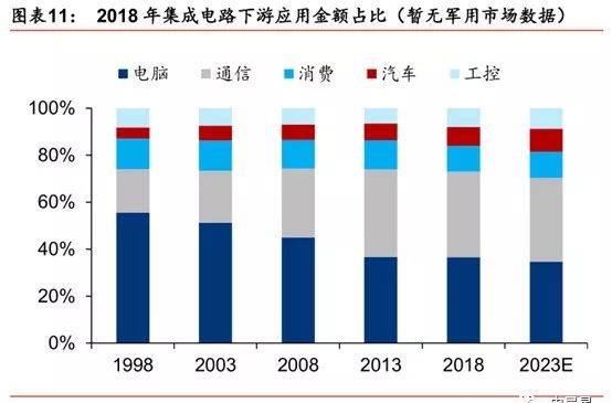
According to IC Insights data, the main downstream applications of integrated circuits in 2018 can be divided into computers (36.6%), communications (36.4%), consumer electronics (11.0%), automotive (8.0%), industrial control (8.0%), and military (6.5%). It is expected that by 2023, the communications market will surpass computers to become the largest downstream market for integrated circuits, with a share likely to reach 35.7%, and the automotive market is expected to increase by 1.8 percentage points compared to 2018.
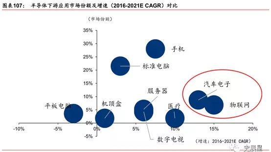
The Internet of Things and automotive electronics are new driving forces for the global semiconductor market’s development.
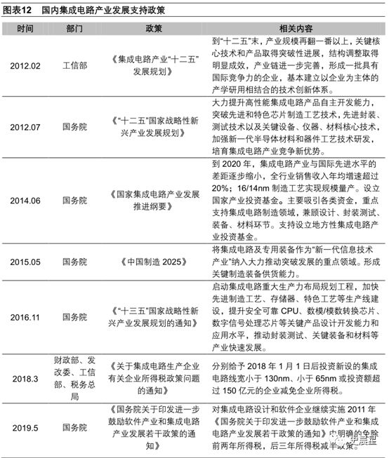
9. Three Major Policies in China
Countries around the world have various supports for the semiconductor industry.
Three Major Policies in China
On June 24, 2014, the National Integrated Circuit Promotion Outline was released, and the National Integrated Circuit Industry Investment Fund was officially established.
Made in China 2025 emphasizes the determination for domestic production.
The project on Large Scale Integrated Circuit Manufacturing Technology and Complete Set of Processes ranks second among the 16 major projects listed in the national major special projects and is known in the industry as the 02 Special Project.
10. Cornerstone of the Information Industry
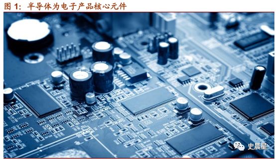
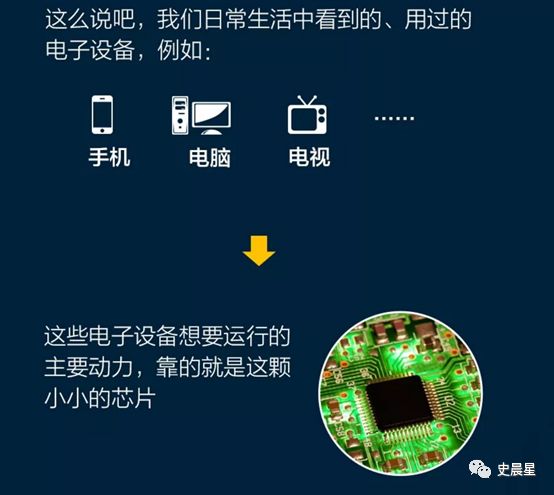
Integrated circuits are referred to as the “grain” of modern industry. In the information age, computers, mobile phones, home appliances, automobiles, high-speed rail, power grids, medical instruments, robots, and industrial control systems all rely on integrated circuits. The United States considers the integrated circuit industry as the foremost of the four technological fields that will fundamentally transform manufacturing in the next 20 years.
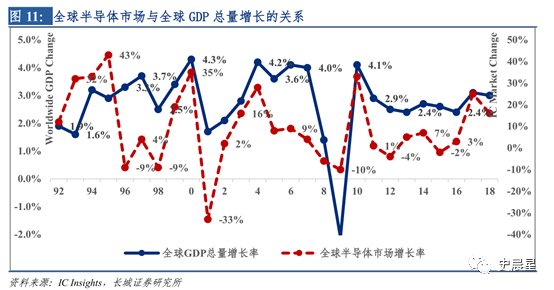
11. Correlation with GDP
The growth rate fluctuations in the global semiconductor industry show a high correlation with global GDP fluctuations (from 2010 to present, the correlation coefficient is 0.57).
12. Trade Deficit Leader
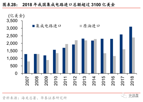
Integrated circuit products have become China’s largest import commodity. According to data from China’s General Administration of Customs, since 2015, the import value of integrated circuits has consistently exceeded that of crude oil, and in 2018, the total import value of integrated circuits in China exceeded 310 billion USD.
13. Bottleneck Issues
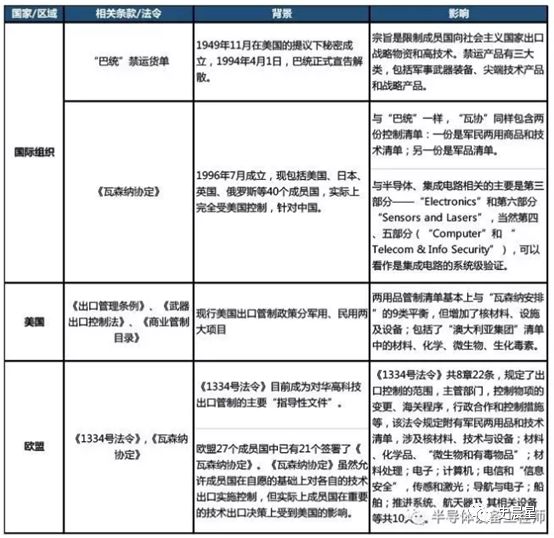
Western countries have formulated a series of technology export restrictions to protect semiconductor technology and have established various review measures for overseas mergers and acquisitions by Chinese companies.
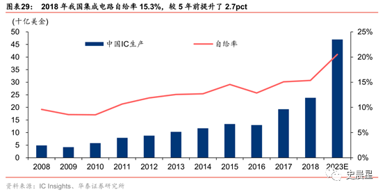
According to estimates from Chip Research, Chinese companies have achieved approximately 17%, 12%, and 6% self-sufficiency in discrete devices, mobile processing, and baseband logic chips, respectively, while other areas still heavily rely on imports.
The severe import dependency in the integrated circuit field affects China’s information security, financial security, defense security, and energy security. The incidents involving ZTE and Huawei have sounded the alarm for us.
Finally, let’s watch a video: Internal Structure of Chips
The comprehensive analysis series of semiconductors consists of three articles, this one is the market analysis, and the next two will be technical and industrial analyses. Please follow this public account (Shichenxing shichenxing1) for updates.
For more content, please click:
PVD Coating Company Resource Library (you can recommend your products for free)
Add to PVD Coating WeChat Group
Job Recruitment
Ion Source Working Principle
Metal Vacuum Surface Modification Technology
Gas Phase Deposition Technology
Common Vacuum Leak Detection Methods
Basic Knowledge of Color Science
Basic Principles of Optical Films
Introduction to Bias Voltage
Metal Processing Technology
Balancing Magnetron Sputtering and Unbalanced Magnetron Sputtering
Scan the QR code to follow us for more surface news