Source: Wisdom Microelectronics
The reason chips are called chips is due to semiconductor technology; the biggest difference between chip systems and board-level systems is the use of semiconductor physical devices. Semiconductor devices are the foundation of chip companies.
Even for chip companies or chip engineers, “semiconductor physics” is a daunting term. This material discusses common semiconductor devices in RF chips.
Introduction to Semiconductor Processes
What is a Semiconductor
Before the discovery of semiconductors, materials in the world were thought to be classified into only two categories based on conductivity: “conductive” and “non-conductive (insulating)”. According to the classification method’s principle of “mutually exclusive and completely exhaustive”, this is a very perfect classification of materials in the world. So why does the classification of “semiconductors” exist?
Some literature defines “semiconductors” as materials with conductivity between conductors and insulators. To be precise, semiconductor materials do not have conductivity characteristics that lie between the two, but rather their conductive properties can be controllably switched between the two.This characteristic of controllable conductivity between conductors and insulators is what defines semiconductor materials.
The phenomenon of semiconductors was first discovered nearly 200 years ago in 1833 when the father of electronics, Faraday, discovered that the resistance of silver sulfide changes with temperature, which is different from that of ordinary metals, allowing for controllable conductivity of silver sulfide material with temperature. This was humanity’s first observation of semiconductor phenomena.
From 1833 to 1945, physicists conducted in-depth research on this phenomenon. The physical revolution of the early 20th century laid a solid theoretical foundation for semiconductor technology, while material growth technology provided the material basis for realizing semiconductor technology.
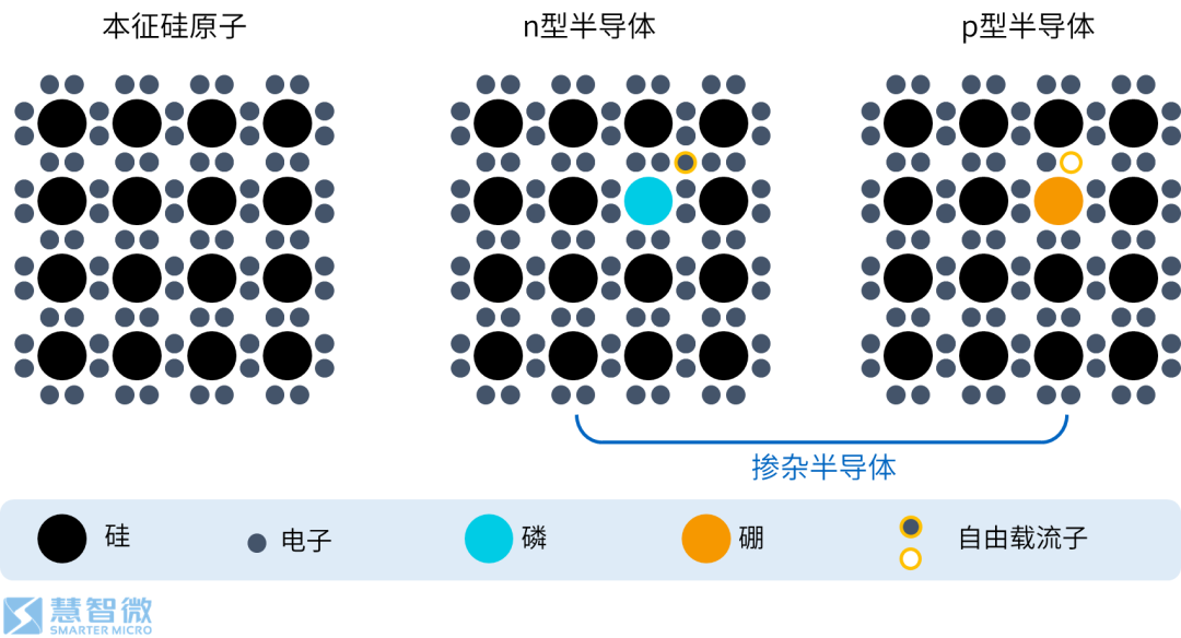
Doping: The Fundamental Basis for Semiconductor Materials
The realization of controllable conductive characteristics in semiconductors is achieved through doping.
Taking silicon atoms as an example, each silicon atom has 4 electrons in its outer shell. In intrinsic silicon material, each silicon atom forms a stable structure with 4 surrounding silicon atoms through covalent bonding, resulting in no freely flowing charge carriers, thus cannot form current.
At this point, if intrinsic silicon material is doped with phosphorus, which has 5 electrons in its outer shell, an extra freely movable electron will be available in addition to the 4 covalent bonds formed, making this electron a free charge carrier. When voltage is applied, the doped material can conduct electricity. The freely moving electron is the first type of carrier in semiconductor materials.
Similarly, if the doping material is boron, which has only 3 electrons in its outer shell, an electron vacancy will appear. As electrons continuously fill this vacancy, the material can also conduct electricity. Because the process of electrons filling this vacancy is difficult to describe, a new way to represent the vacancy was invented, defining a new carrier to represent this vacancy. This new carrier is the second type of free charge carrier in semiconductors: holes.
The doping process in semiconductors achieves control over free charge carriers within the material.
p-n Junction: A Simple Semiconductor Device
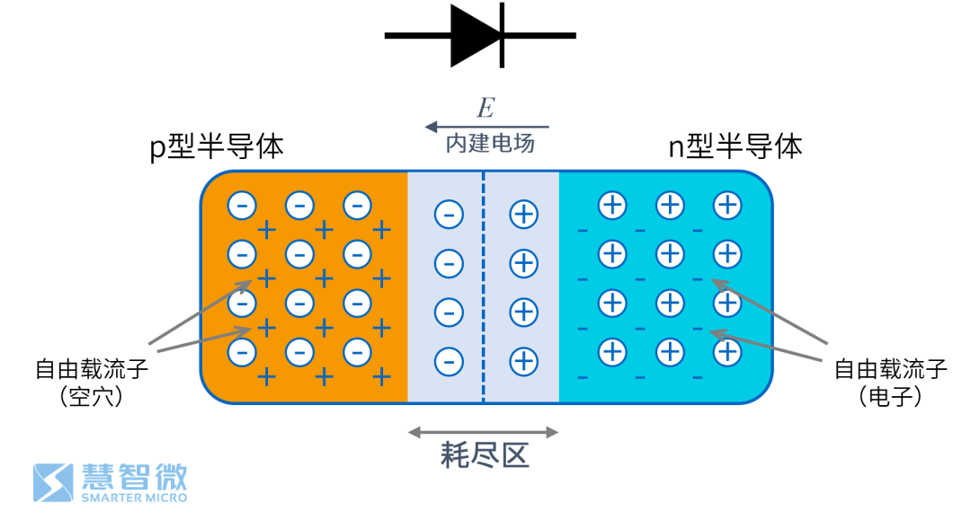
Figure: Basic structure of a p-n junction
Using the doping characteristics of semiconductors, a simple semiconductor device can be designed: the p-n junction. The p-n junction, in English, is called the p-n Junction, and due to its positive and negative ports, it is also referred to as a p-n junction diode.
The p-n junction is formed by simultaneously doping p-type and n-type materials on the same substrate, creating a depletion region (also known as the space charge region) at their junction, thus forming the p-n junction.
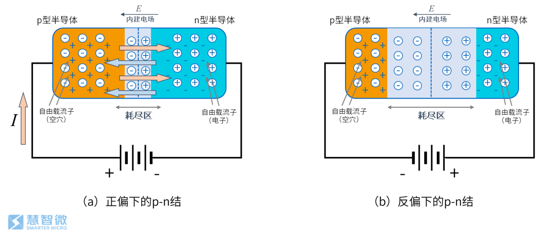
One important characteristic of the p-n junction is its unidirectional conduction property. When a positive voltage is applied to the p-type semiconductor side, the holes in the p-type semiconductor move to the right under the influence of the external electric field. When the external electric field exceeds the built-in electric field of the p-n junction, the holes will cross the depletion region and enter the n-type semiconductor region, subsequently flowing to the negative terminal of the power supply, forming current.
When a positive voltage is applied to the n-type semiconductor side, the free charge carriers (electrons) in the n-type semiconductor move to the right, widening the built-in electric field, making it more difficult for free charge carriers to cross the depletion region, thus preventing current from forming.
Figure: p-n junction under forward and reverse bias
From “Transistor” to Changing the World
However, using just the p-n junction diode is not sufficient for designing integrated circuits.
Once the basic principles of semiconductor physics were mastered by humanity, people began to design and manufacture special devices using semiconductor materials. For example:
-
By utilizing the relationship between semiconductor conductivity and temperature, thermistors can be designed to sense temperature changes;
-
By utilizing the relationship between some semiconductors’ conductivity and light, light-sensitive resistors can be designed to sense changes in light;
-
By utilizing some semiconductor photoelectric conversion characteristics, devices can be designed to convert electrical energy and light energy, such as light-emitting devices or photovoltaic devices;
Although important application devices can be designed in many fields using the controllable conductivity characteristic of semiconductor materials, semiconductors during this period were still very difficult to connect with the “integrated circuits” that would later change the world. The real connection between “semiconductor materials” and “integrated circuits” was established with the invention of the “transistor” in 1945.
As early as 1899, humanity managed to transmit radio signals across the English Channel. However, before the invention of the transistor, electronic circuit systems were generally designed using vacuum tubes. Vacuum tubes are large, consume a lot of power, generate a lot of heat, have short lifespans, and require high-voltage power supplies, so circuits designed with vacuum tubes were typically only used in government and military departments. Vacuum tubes greatly limited the large-scale application of circuit systems.
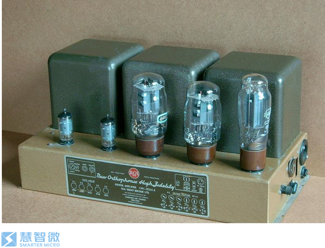
Figure: Amplifier designed by RCA using vacuum tubes in the early 20th century
To overcome the limitations of vacuum tubes, after World War II, Bell Labs accelerated research to explore the possibility of making amplifying devices using semiconductor materials.
In the fall of 1945, Bell Labs established a semiconductor research group led by Shockley, with members including Brattain and Bardeen. They discovered that by connecting electrodes to the bottom of a germanium wafer and inserting a fine needle into one side while applying current, and then bringing another fine needle close to and touching it while applying a weak current, the original current would change significantly.
A small change in weak current can have a significant impact on another current, which is the “amplification” effect. Using this characteristic, semiconductor devices can also be used to make amplifiers.
When naming this device, Brattain thought of its resistance-changing characteristics, thus naming it Trans-resistor (transforming resistor), which was later abbreviated to Transistor; the Chinese translation is 晶体管 (Jīngtǐguǎn).In 1956, Shockley, Bardeen, and Brattain jointly received the Nobel Prize in Physics for inventing the semiconductor transistor.
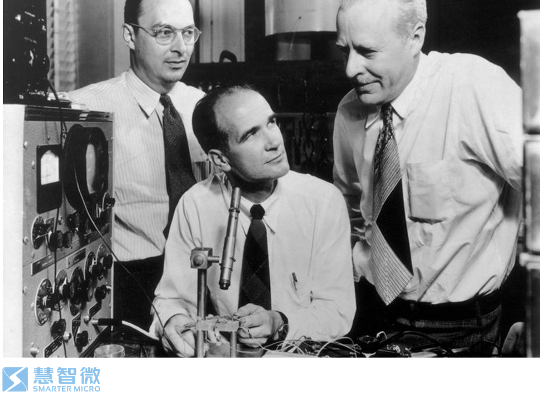
Figure: Inventors of the semiconductor transistor, from left: Brattain, Shockley, Bardeen
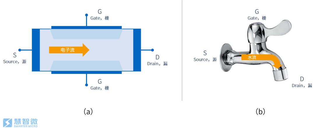
In intuitive understanding, a transistor can be likened to a faucet:
-
A transistor has three terminals; for FET devices, they are generally called source, drain, and gate (S, D, G), corresponding to the inlet, outlet, and handle of the faucet;
-
The source terminal (Source) of the transistor flows in electrons, corresponding to the water flowing into the faucet;
-
The gate (Gate) is the core of the transistor, controlling the amount of current, corresponding to the handle of the faucet, which determines the strength of the water flow;
Figure: Typical transistor structure (JFET), and its equivalent to a faucet
Based on the above principles, transistors can achieve signal amplification. By applying a small signal at the gate, as long as the on/off state of the channel between the drain and source can be controlled, the current size between the drain and source can be controlled.
Transistors can also represent the basic signals “0” and “1” in digital circuits. For example, the open state of the “faucet” can be defined as “1”, and the closed state as “0”. When thousands of such “faucets” are put together, digital logic operations can be performed.
The transistor (Transistor) is the most important basic device in the field of integrated circuits, without exception. It is this basic device that has led to the integrated circuits that have changed the world today.The last letter “T” in the names of devices we often see, such as FET, HBT, pHEMT, etc., is an abbreviation for “Transistor”.
In semiconductor devices, transistors also have various forms, materials are diverse, and some abbreviations can be overwhelming. However, regardless of the variation, as long as the “inlet” and “outlet” of the faucet in the transistor are identified, and the working principle of the “handle” is understood, this type of transistor can be analyzed clearly.
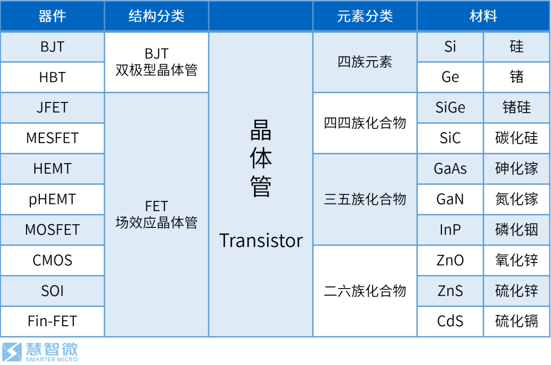
Classification of Transistors
In the nearly 100 years of development of semiconductor transistors, pioneering scientists and engineers have continuously experimented with various device structures and materials to meet the needs of different fields of integrated circuit characteristics, resulting in a wide variety of semiconductor devices.
Semiconductors are inherently abstract and elusive, and the myriad names and abbreviations make semiconductors even more esoteric, causing considerable confusion for professionals in the electronics industry who do not come from a semiconductor background.
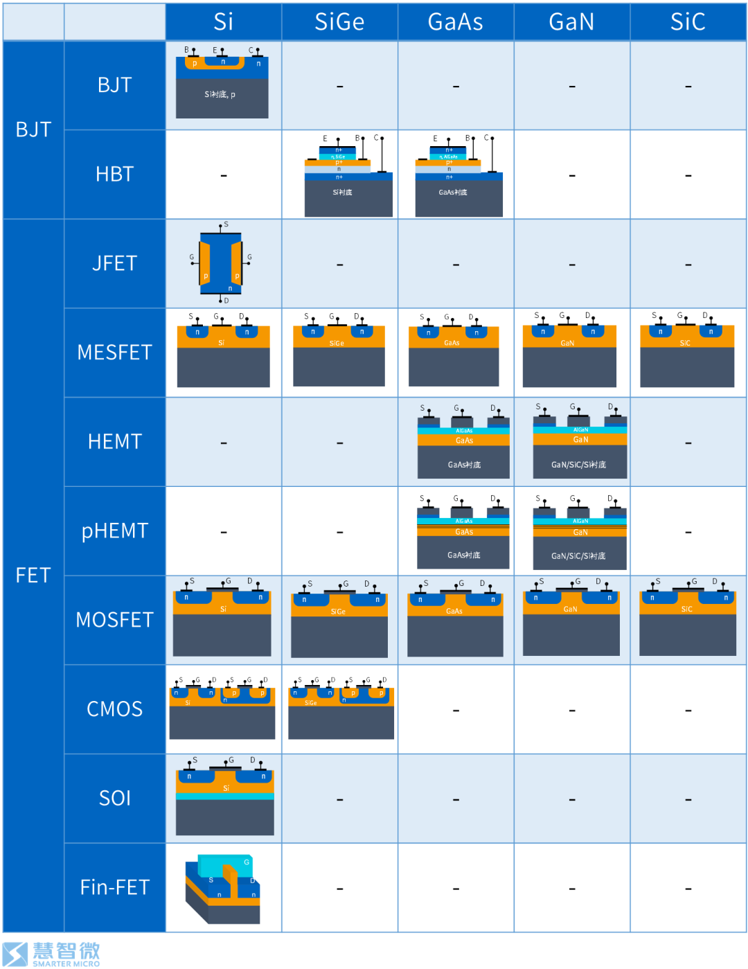
Transistors can be classified mainly in two ways: by device structure and by device materials. Below are common structural and material types.
The materials and structures of transistors are independent of each other and can theoretically combine freely. For example, BJT devices can be designed on silicon substrates, or BJT devices can be designed on gallium arsenide substrates.
To accurately describe a device, both the material and the type of device should be specified. For example, for the HBT device used in the 5G mobile phone RF PA, the accurate name should be GaAs HBT device. However, due to common conventions in daily work, the naming is often simplified.
For instance, in the mobile RF field, people generally use HBT or GaAs to refer to GaAs HBT; in the power control field, SiC is used to refer to SiC MOSFET, and GaN is used to refer to GaN FET devices. Such abbreviations are effective in a specific sub-industry, but when communicating outside of that industry, they may cause misunderstandings, which should be noted when necessary.
Classifying Semiconductors by Structure
From a structural perspective, semiconductor devices are mainly divided into two types: BJT and FET.
BJT stands for Bipolar Junction Transistor, while FET stands for Field Effect Transistor. Both can achieve the amplification characteristics of transistors.
BJT Devices
Basic Structure
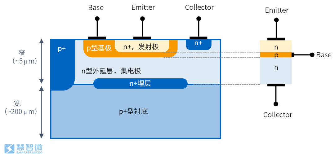
BJT devices consist of two back-to-back p-n junctions. Since the p-n junction used for current transmission contains both electrons and holes as charge carriers, the BJT device is named “Bipolar Junction Transistor”.
Although BJT consists of two p-n junctions, not just any two back-to-back p-n junction diodes can form a BJT. BJT devices have precise requirements for the doping concentrations and thicknesses of each region. The emitter region in a BJT device needs to be heavily doped, the base region needs to be moderately doped, and the width must be very thin to allow a large number of electrons and holes to traverse.
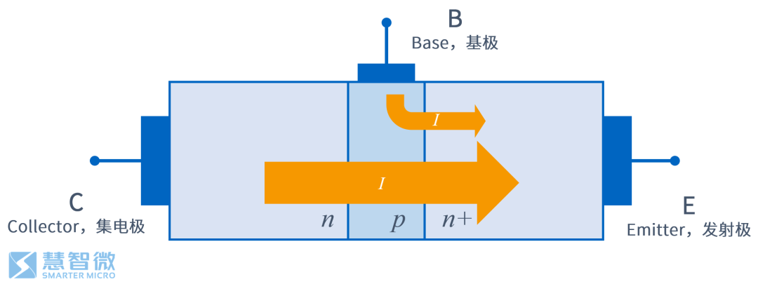 Figure: Basic structure of a BJT device (example of npn transistor)
BJT Device Fabrication
In integrated circuit fabrication, BJT devices are first formed by creating a p-type diffusion in n-type epitaxy to form the base; then n-type diffusion is performed to form the emitter, thus achieving the two adjacent p-n junctions.
As shown in the figure, in a BJT device, the current flows in the vertical direction, so BJT devices in integrated circuits are vertical devices.
Figure: BJT device cross-section and simplified model
HBT: A Special BJT Device
HBT stands for Heterojunction Bipolar Transistor, a special type of BJT device.
The improvement of HBT over ordinary BJT is the use of different semiconductor materials between the emitter and base to form a heterojunction p-n junction, which helps to resist the injection of base charge carriers into the emitter, allowing more charge carriers in the emitter to flow into the collector region, thus increasing the current from collector to emitter. The observed phenomenon is that the base current decreases while the collector current increases, giving the base current stronger control over the collector current.
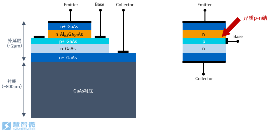
Common HBT devices include GaAs HBT devices and SiGe HBT devices. The following figure shows a typical cross-section of a GaAs HBT device.
Figure: Cross-section and simplified model of GaAs HBT device
AlGaAs/GaAs is the most widely studied and applied heterojunction system. The GaAs HBT used in 5G RF PA is of this type of heterojunction HBT. In the AlGaAs/GaAs heterojunction HBT, a thin film of n-type Al0.3Ga0.7As is injected between the p+ GaAs layer of the base and the n+ GaAs emitter, forming a heterojunction p-n junction between the base and emitter.
Epitaxial Layer: The Key Material of HBT Devices
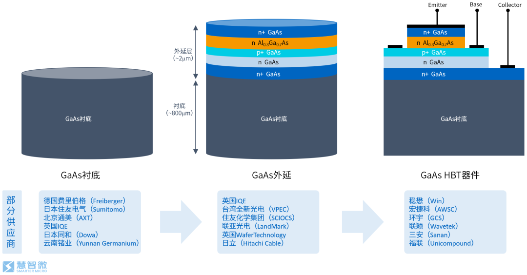
The structure of HBT devices can be seen to consist of an epitaxial layer and a substrate.
In integrated circuits, wafer fabrication includes two major processes: substrate preparation and epitaxial growth. The substrate is a wafer made of single crystal semiconductor material, which can directly enter the wafer manufacturing process to produce semiconductor devices or go through epitaxial growth to create the epitaxial layer before proceeding to semiconductor device manufacturing.
Epitaxy (Epitaxy, abbreviated as Epi) refers to the process of growing a new single crystal on a single crystal substrate. Since it grows on the substrate, it is called “epitaxy”. The epitaxial layer is generally only a few micrometers thick, and the new single crystal can be the same material as the substrate or a different material.
The epitaxial process solves the problem of devices only being able to use one substrate material, making it possible for different regions of the device to use different materials, greatly increasing the flexibility of device design. For HBT devices, since it is necessary to design AlGaAs/GaAs heterojunction p-n junctions, it is necessary to use epitaxial layer processes to design different materials and doped semiconductor material layers.
By designing different epitaxial layers, the characteristics of HBT devices can also be adjusted. The performance of HBT devices depends on the thickness and doping concentration curves of the emitter, base, and collector in the device, and these data are adjusted during the design of the epitaxial layer.
In the production chain of HBT devices, GaAs substrates are generally produced by substrate manufacturers, then handed over to epitaxial manufacturers to grow the epitaxial layer, and finally delivered to foundries for HBT device production. Since the material parameters of the semiconductor devices in the epitaxial layer are already determined, the growth of the epitaxial layer is a key step in the production of HBT devices.
Figure: GaAs HBT device production chain process
FET Devices
FET devices stand for Field Effect Transistor. The term Field Effect refers to using an electric field to control the flow of current within the semiconductor.
The idea behind FET is very simple and direct: by adding a different type of doped semiconductor material (such as n-type) on both sides of a doped semiconductor material, and controlling the voltage on the p-type doping, the conduction or cutoff of the n-type channel can be controlled, thus achieving the purpose of controlling current. The working principle of FET is even more intuitive, resembling a faucet.
In FET devices, only one type of charge carrier (such as electrons in n-channel FET devices) participates in conduction, which is very different from BJT devices where both electrons and holes participate in conduction. Therefore, the earliest FET devices were also called Unipolar Transistors, emphasizing this single charge carrier conduction characteristic.
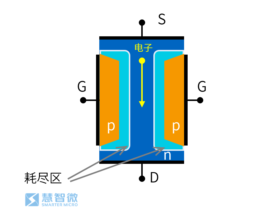
In n-channel FET devices, there are three terminals: the source terminal (Source, S), which provides electrons; the drain terminal (Drain, D), which drains electrons; and the gate terminal (Gate, G), which controls the channel.
Figure: Principle diagram of FET devices
Compared to the complex p-n junction operation theory of BJT devices, the concept of FET devices is simple and direct, focusing on “channel” and “cutoff”, which aligns well with human intuition. Therefore, the idea of FET was proposed even before BJT was commercialized.
In 1926, J. E. Lilenfeld filed a patent application that first proposed the concept of FET, which was 21 years earlier than the invention of BJT devices by Shockley’s team at Bell Labs in 1947. However, due to the limitations of technology at the time, FET devices only existed as concepts in the minds of early scientists. It wasn’t until 1953, thanks to advancements in technology, that FET devices were actually produced. The first FET device to be produced was the JFET (Junction FET) device.
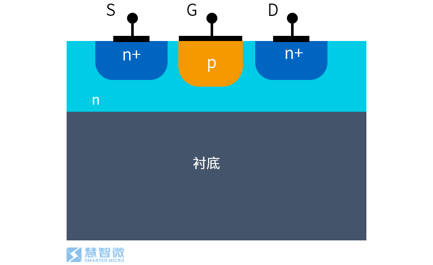
JFET
JFET is the first FET device to be officially produced. Because the name includes “Junction”, it also utilizes the characteristics of p-n junctions in its operation.
Figure: Structure and working principle of JFET
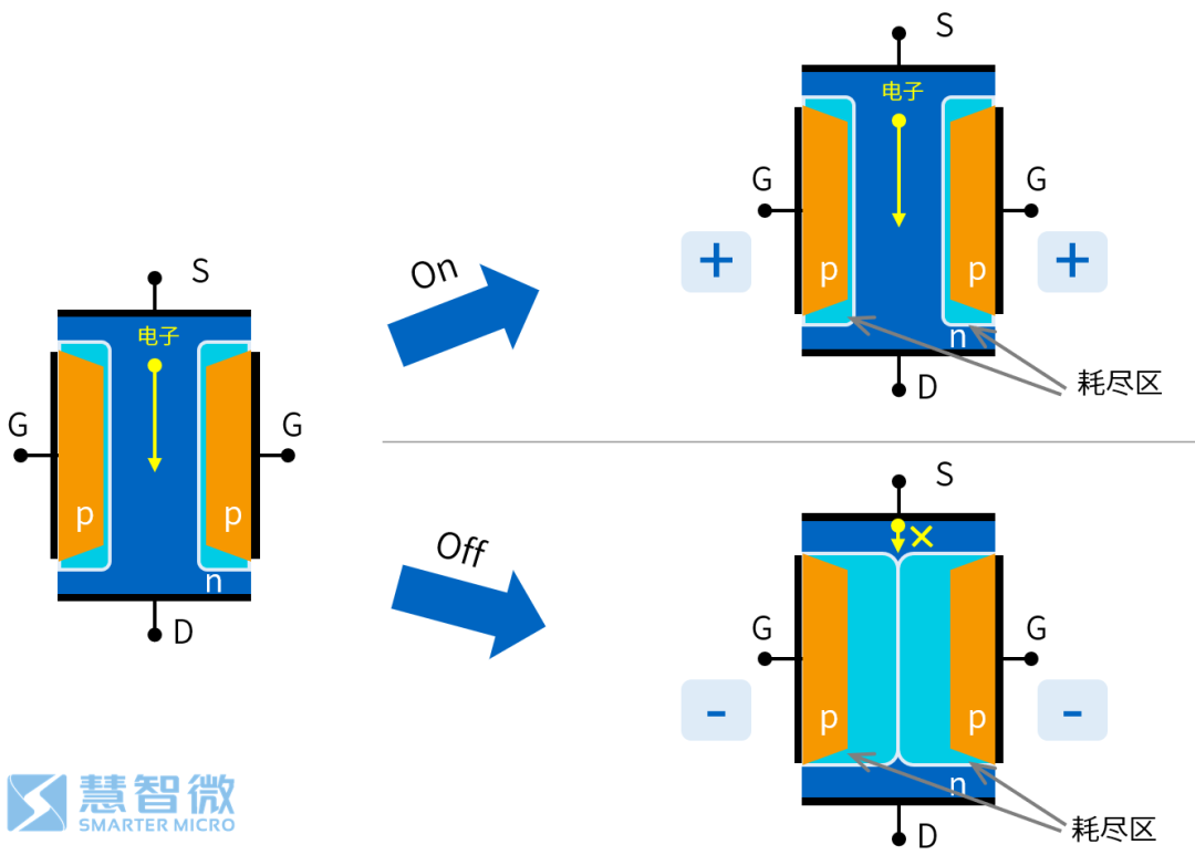
JFET was first proposed and analyzed by Shockley’s team in 1952. In JFET, the applied gate voltage changes the width of the depletion layer of the p-n junction, thereby changing the conductivity between the source and drain.
After years of technological advancements, the structure of JFET has also changed. The following figure shows the modern JFET structure, which, although different in physical appearance from the earliest JFET, still uses electric field control of the gate p-n junction, equivalent to the original Shockley structure.
Figure: Modern epitaxial layer JFET device structure
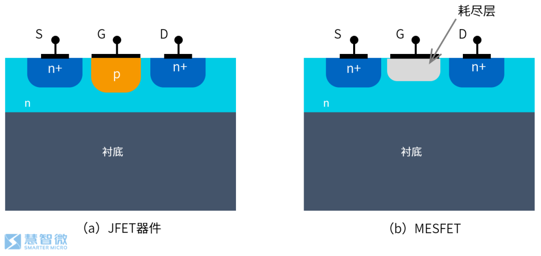
MESFET
MESFET stands for Metal-Semiconductor FET. MESFET is a transistor developed using the characteristics of metal-semiconductor contact. The structure of JFET and MESFET is compared below.
Figure: Comparison of structures between JFET and MESFET
The working principle of MESFET is similar to that of JFET, with the only difference being that the controlling of the channel cutoff is no longer done by a p-n junction, but rather by a metal-semiconductor junction (referred to as a metal-semiconductor junction).
Metal-semiconductor contact is a very important area of research in semiconductor theory, and it has broad applications in many semiconductor devices. The study of metal-semiconductor contact began with the establishment of semiconductor physics theory in 1874, and in 1938, Schottky completed the theory of metal-semiconductor barrier, forming the theoretical system. Thus, the metal-semiconductor contact that forms a Schottky barrier is also called Schottky contact, and the diodes developed from it are called Schottky diodes. In addition to Schottky contacts, metal contacts with heavily doped semiconductors can also form ohmic contacts, which are necessary for all semiconductor devices to flow in and out.
The commercially widely used MESFET device is the GaAs-based MESFET, which, due to the electron transport characteristics of GaAs, has excellent RF performance and is the core of today’s monolithic microwave integrated circuits (MMIC).
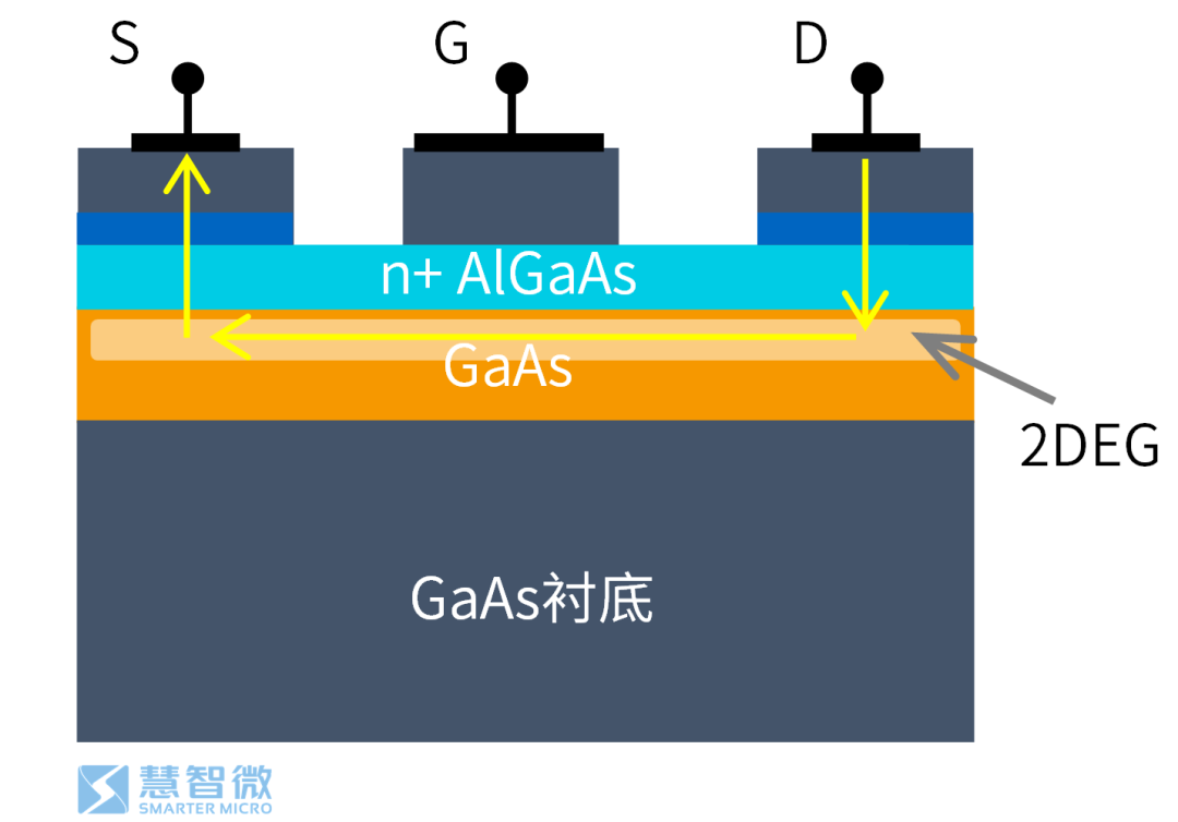
HEMT and pHEMT
HEMT stands for High Electron Mobility Transistor. HEMT devices were first invented by Fujitsu in Japan in 1979. The idea behind HEMT devices is to utilize the characteristics of heterojunctions of different semiconductor materials to gather a large number of electrons at the junction, forming a high mobility layer known as “two-dimensional electron gas (2DEG)”, achieving better device performance. HEMT devices have irreplaceable applications in high-frequency millimeter-wave fields and low-noise applications.
Because it utilizes heterojunctions, HEMT is also referred to as heterostructure FET (HFET). The following figure shows a typical structure of HEMT devices.
Figure: Typical structure of HEMT devices
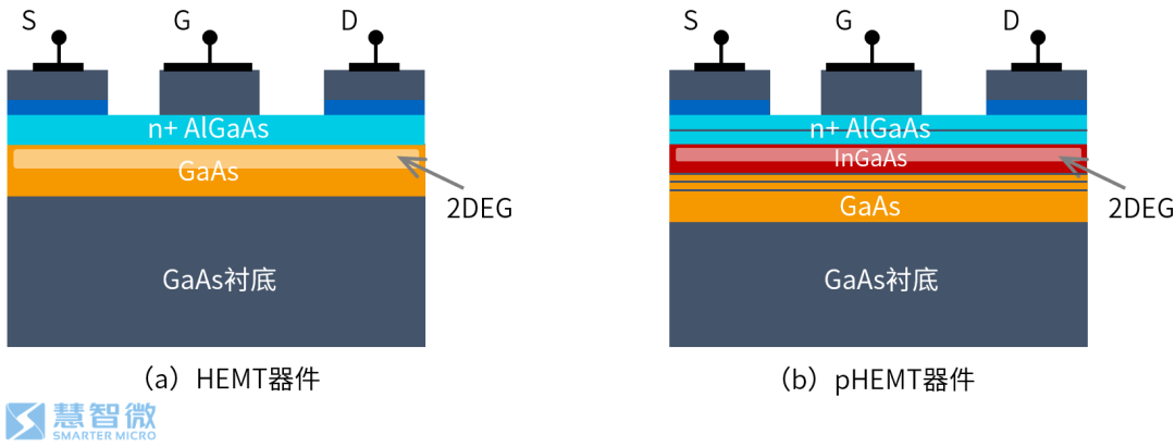
Under normal circumstances, there will be lattice mismatches at the heterojunction contact surface, which will affect device performance and the selection of materials with larger bandgap voltages. This led to the development of an improved version of the HEMT device: pHEMT.
pHEMT stands for Pseudomorphic HEMT. Pseudomorphic means fake or pseudo-matched, and the pHEMT device adds a thin “pseudomorphic layer” during the heterojunction transition to pull the lattices on both sides toward matching.
Figure: Structural diagram of HEMT and pHEMT devices
Due to their excellent RF performance, pHEMT devices are widely used in high-performance RF microwave fields. In particular, GaAs pHEMT devices are important semiconductor processes for microwave low-noise amplifiers and microwave millimeter-wave circuits.
Similar to HBT devices, the characteristics of HEMT and pHEMT devices strongly depend on material properties. In the HEMT/pHEMT production chain, it is also necessary for epitaxial layer manufacturers to produce the corresponding material epitaxial layers, which are then processed into devices by foundries.
MOSFET
MOSFET structure is undoubtedly the core structure in today’s integrated circuit field.
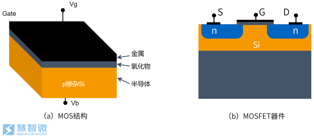
MOSFET stands for Metal-Oxide-Semiconductor FET, and MOSFET is a special structure of MIS (Metal-Insulator-Semiconductor) devices. The following diagram shows a typical MOS structure and a schematic of MOSFET.
Figure: MOS structure and MOSFET device structure
Before the advent of MOSFET, there were already planar MESFET devices and vertical BJT devices, but neither of these circuits could adapt to large-scale circuit design:
-
The vertical structure of BJT devices cannot achieve effective integration; the working mechanism of BJT devices makes it impossible to effectively turn off or on the device; the current at the Base terminal also causes BJT devices to have a large operating current.
-
Although MESFET is a planar device, solving the integration problem, the metal-semiconductor junction used in MESFET devices clamps too large a Gate voltage, causing Vg to only be usable within a certain range.
Thus, the MOSFET device was invented.
The modern MOSFET device was proposed in 1960 when Ligenza and others proposed a MOSFET device based on the Si-SiO2 structure, addressing a series of shortcomings of MESFET and suitable for large-scale integration and proportional size reduction. From then on, semiconductor devices were no longer individual transistors, and the curtain of large-scale integrated circuits was raised.
Various semiconductor structures based on MOSFET devices include CMOS, SOI, Fin-FET, etc.
CMOS
The invention of CMOS circuits propelled integrated circuits into the fast lane of “proportional reduction”, marking a significant leap in the history of integrated circuits.
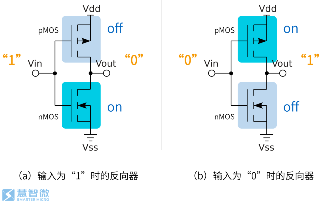
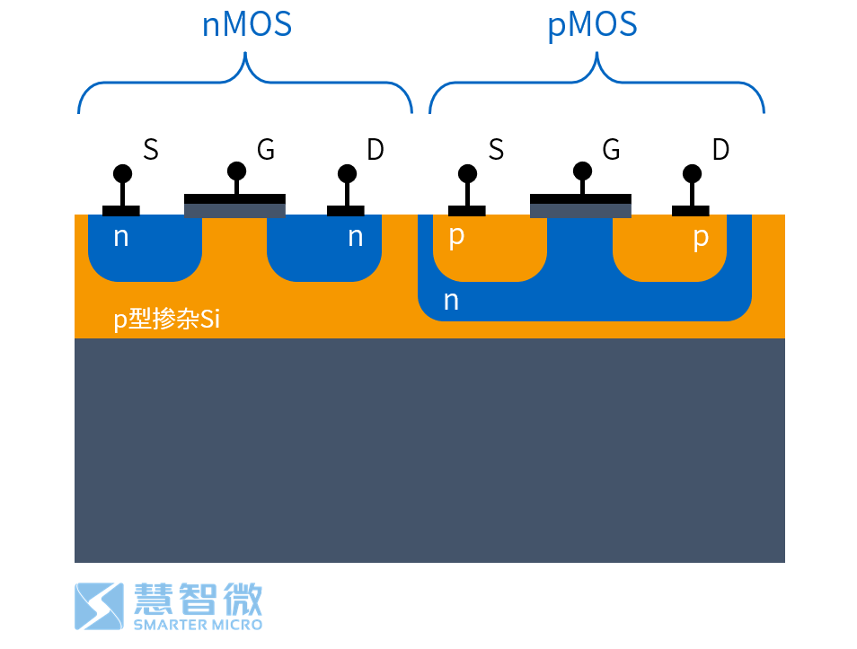
CMOS stands for Complementary metal–oxide–semiconductor, meaning the circuit consists of not only nMOS but also pMOS. By combining two types of MOS devices, digital integrated circuit logic circuit design can be perfectly completed.
Although BJT devices can also be used to design similar TTL (Transistor-Transistor Logic), the advantage of CMOS logic lies in its low static power consumption. For example, in a simple inverter circuit, at any given time, only one device in the pathway (nMOS or pMOS) is conducting, resulting in a theoretical static power consumption of 0.
Figure: Explanation of the working principle of CMOS inverter
CMOS devices were invented in 1963 at Fairchild Semiconductor and were subsequently applied to digital circuit designs such as storage and processors.
Figure: Basic structure of CMOS devices
After the invention of CMOS devices, people found that this technology perfectly complemented digital circuit technology. Digital circuits require basic logic units that are small in size and low in power consumption, and CMOS devices can meet this demand perfectly. Thus, humanity continuously improved semiconductor processes to reduce the size of CMOS devices, making digital circuits increasingly powerful.
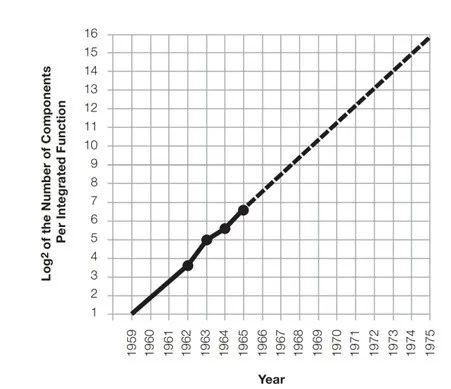
In 1965, Gordon Moore of Fairchild Semiconductor published a brief article in Electronics Magazine, predicting that the number of transistors that could fit on an integrated circuit would double approximately every 18 to 24 months from 1965 to 1975. In other words, processor performance would roughly double every two years, while the price would drop to half of what it was before.
What gave Moore the confidence to make this prediction was the expectation of CMOS technology.
Figure: Gordon Moore’s “Moore’s Law” proposed in 1965
However, what Gordon Moore did not expect was that the validity of Moore’s Law would not be limited to the 10 years he anticipated from 1965 to 1975, but would support the development of the entire integrated circuit industry for nearly 60 years. During these 60 years, the number of transistors on processors increased from hundreds to billions or even tens of billions, and the feature size of CMOS devices shrank from several millimeters to several nanometers. In the Qualcomm 8 series smartphone platform chip released, a 4nm process was used, integrating nearly 20 billion transistors. A small integrated circuit has gained unparalleled powerful functionality.
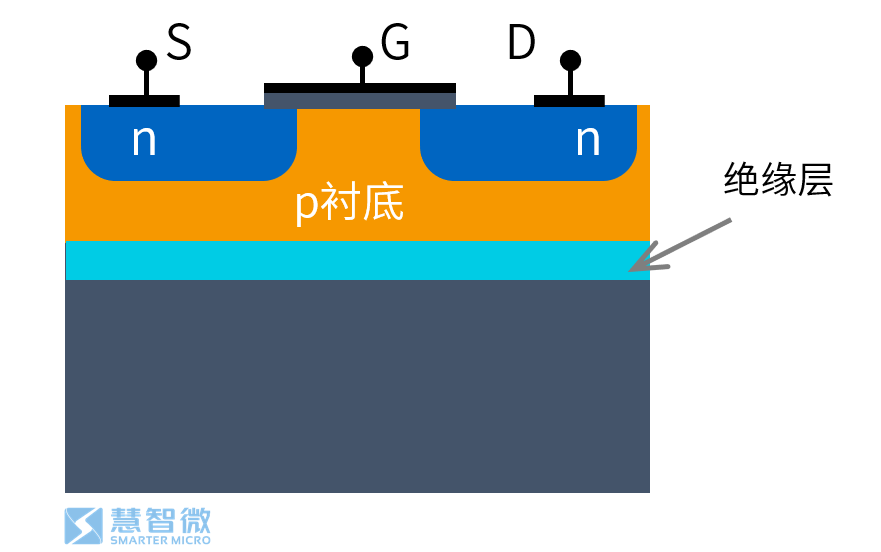
SOI
SOI stands for Silicon on Insulator, which refers to the technology of producing semiconductor devices on silicon substrates with an insulating layer. SOI technology can reduce the impact of substrate losses on device performance, resulting in better device characteristics. The semiconductor devices produced using SOI technology are shown in the figure below.
Figure: Basic structure of SOI devices
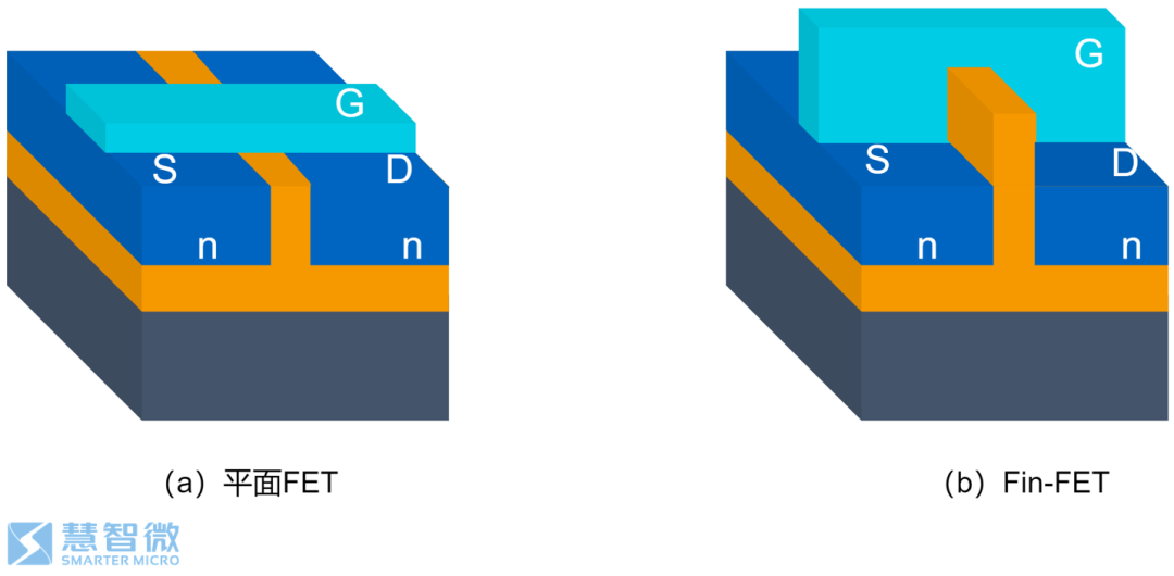
Fin-FET
Fin-FET, named for its fish fin-like shape, is a device structure invented to continuously reduce device size under the drive of Moore’s Law.
Before the invention of Fin-FET, as device sizes continued to shrink due to Moore’s Law, the original planar gate structure could no longer effectively control the device channel, leading to significant leakage current. Thus, Professor Zhenming Hu from the University of California, Berkeley, proposed the Fin-FET structure in 1999, which upgraded the gate structure from planar to a fish fin-like three-dimensional structure, resulting in better control over the channel.
Figure: From planar CMOS FET to Fin-FET
Currently, TSMC, Intel, Samsung, and others use Fin-FET for advanced CMOS process design.
Classifying Semiconductors by Material
In addition to classification by device type, semiconductors can also be classified by material.
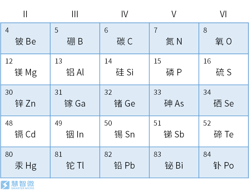
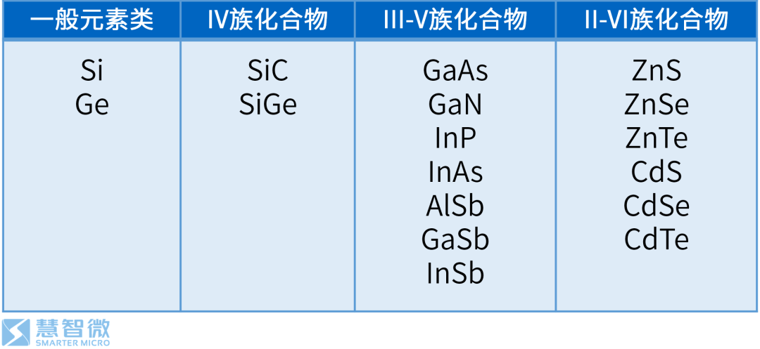
There are many types of semiconductor materials used to make semiconductors, not only silicon materials that we are familiar with but also germanium. Additionally, compound materials such as GaAs, GaN, SiC, etc., are also common semiconductor materials. The table below lists some elements in Group II-VI of the periodic table, which can form typical semiconductor materials.
Figure: Common elemental materials used in semiconductors
Common semiconductor materials made from the above elements include:
It should be noted that there are many materials used for semiconductors, and even within a single semiconductor device, different semiconductor materials may be present. When naming a device, it is generally based on the material that constitutes the important part of that semiconductor device (such as the channel).
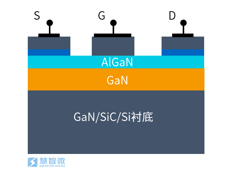
For example, for the GaN HEMT device shown below, although the device can be grown on Si or SiC substrates, the channel of the device is made of GaN, and the heterostructure of GaN and AlGaN, so the device is referred to as a GaN HEMT device or AlGaN/GaN HEMT device.
Figure: Schematic diagram of GaN/SiC/Si-based GaN HEMT device
Combining Materials and Structures
As mentioned at the beginning of the article, the combination of materials and device structures is essential for accurately describing devices. The complete device name should be “material + device structure”.
Theoretically, different materials and device structures can combine freely. However, due to material characteristics and specific requirements, it is not possible to grow any type of device on all materials. In practice, the main combinations of materials and structures for devices are as follows.
Figure: Semiconductor devices with different materials and structures
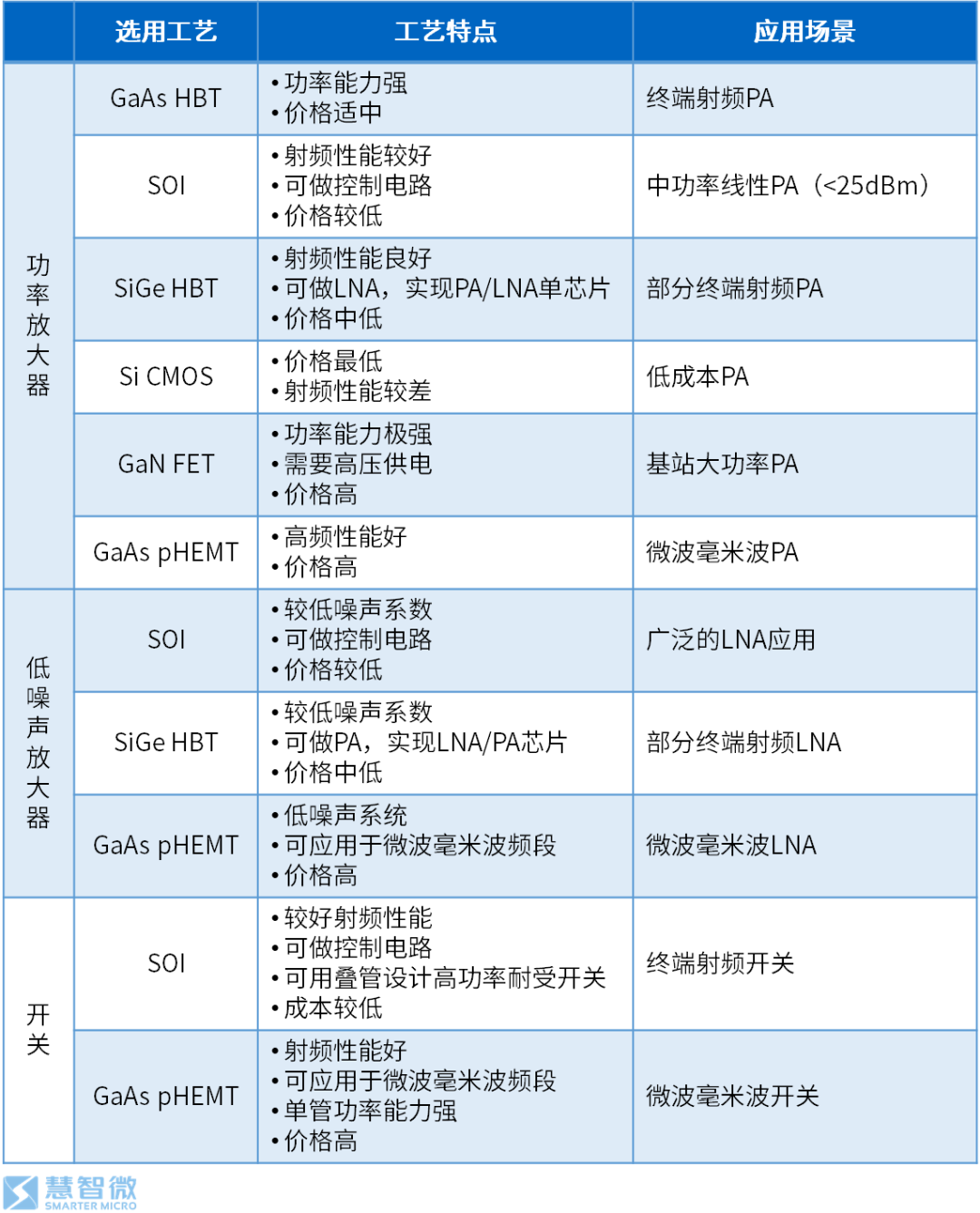
Semiconductor Devices in 5G RF
In the design of RF front-end chips, various semiconductor processes are also required. The semiconductor processes commonly used in various RF front-end modules and their characteristics are summarized as follows:
66 years ago, the world’s first semiconductor transistor was born at Bell Labs. Since then, with the development of semiconductor processes and the invention of integrated circuits, small semiconductor devices have transformed every aspect of human life.
RF technology has also been greatly influenced by semiconductor technology. Whether in the module chips used in mobile terminals or the semiconductor tubes used in base stations, semiconductor devices, as core components, have become the foundation of today’s RF technology.
However, semiconductor technology is abstract, and semiconductor devices are complex; often, they cannot be directly related to daily use, causing considerable confusion in everyday work.
This article organizes the types of semiconductor devices commonly seen in various RF modules, hoping to assist everyone in their work when needed.
[1].Lilienfeld, J.E. “Method and apparatus for controlling electric current” US Patent no. 1,745,175 (filed: 8 October 1926; issued: 28 January 1930).
[2].Ligenza J R, Spitzer W G. The mechanisms for silicon oxidation in steam and oxygen[J]. Journal of Physics and Chemistry of Solids, 1960,14:131-136.
[3].”1963: Complementary MOS Circuit Configuration is Invented”. Computer History Museum. Retrieved 6 July 2019.
[4].Moore, Gordon E. (1965-04-19). “Cramming more components onto integrated circuits” (PDF). intel.com. Electronics Magazine. Retrieved April 1, 2020.
[5].S. M. Sze, Physics of Semiconductor Devices.
This content is reprinted and only represents the author’s views
It does not represent the position of the Institute of Semiconductor, Chinese Academy of Sciences
Editor: Lu Dingci