
Source: Power Semiconductor Insights

Semiconductor materials have unique electrical and physical properties, allowing semiconductor devices and circuits to perform specific functions. The progress of semiconductor localization is ongoing, and as someone in the related industry, I am continuously learning and accumulating knowledge. The following discussion will mainly focus on semiconductor chips, and I hope everyone enjoys it~

From materials to devices, and from devices back to materials, there are countless steps involved, leading to various career positions. The inability to have a comprehensive understanding might be a frustration after entering the workforce as a “worker.” I hope the upcoming content will help everyone understand the intricacies of semiconductors. Today, we will discuss a few fundamental concepts about semiconductor materials.


Everything is composed of 96 stable elements and 12 unstable elements, each with a different atomic structure, which determines the distinct properties of the elements. Further breaking down atoms reveals three subatomic particles: protons, neutrons, and electrons, each with its own characteristics, and different combinations and structures lead to different atomic properties.
The first to use the basic structure of atoms to explain the unique physical, chemical, and electrical properties of different elements was Danish physicist Niels Bohr:
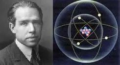
Image source: Baidu Encyclopedia
In Bohr’s atomic model, positively charged protons and neutral neutrons are concentrated in the nucleus, while negatively charged electrons orbit around the nucleus, forming a relatively stable atomic structure, similar to planets revolving around the sun.
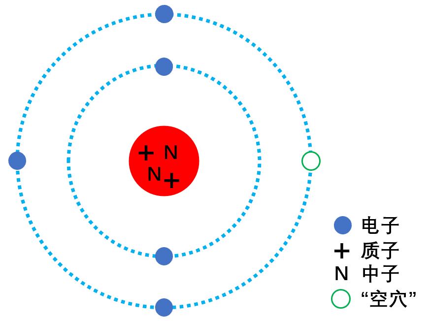
Each orbit can only accommodate a limited number of electrons, and in some atoms, not every position will be filled with electrons, leaving an empty position—hole. Once an electron orbit is filled, the remaining electrons must occupy the next layer’s orbit.


An important property of many materials is conductivity, which is the ability to support electric current. The essence of electric current is the flow of electrons. If the protons in an element or material have a relatively weak grip on the outer electrons, electric conduction can occur, allowing these electrons to easily establish an electric current, a situation common in most metals.
Conductivity is generally represented by conductivity, and the higher the conductivity, the better the material’s conductive performance. The reciprocal of conductivity is known as resistivity, and the lower the resistivity, the better the corresponding conductive performance.In contrast to conductivity is insulation, where some materials exhibit a strong grip of the nucleus on the orbiting electrons, significantly hindering their movement. For example, silicon dioxide is used as an insulating material in semiconductors.
A sandwich structure with an insulating layer sandwiched between two conductors is known as a capacitor. In semiconductor structures, many “sandwich” structures exist, which we commonly refer to as parasitic capacitance. Capacitors are used in storage devices for information storage, eliminating detrimental charges accumulated on the conductors and silicon surface, and forming functional devices in field-effect transistors. Semiconductor metal conduction systems require high conductivity, thus necessitating materials with low resistance and low capacitance. These materials are insulators with low dielectric constants, while the insulating layers used for interlayer isolation require high capacitance or high dielectric constant insulators.


Semiconductor materials, as the name implies, are materials that inherently possess some natural conductivity. The two main semiconductor materials are silicon (Si) and germanium (Ge), along with dozens of other compound semiconductor materials, which are materials made from two or more elements.
“Intrinsic” refers to materials in a pure state without impurities. Intrinsic semiconductors are pure semiconductors without any impurities or lattice defects. However, the semiconductors we use are not intrinsic but are doped semiconductors created through a doping process, which introduces specific elements into intrinsic semiconductors to enhance their conductivity, exhibiting two characteristics:
① Precisely controlling resistivity through doping;
② Conductivity through electrons and holes.
Doping allows semiconductor materials to achieve a useful range of resistivity, categorized into n-type and p-type semiconductors. The following graph illustrates the relationship between doping level and silicon resistivity:
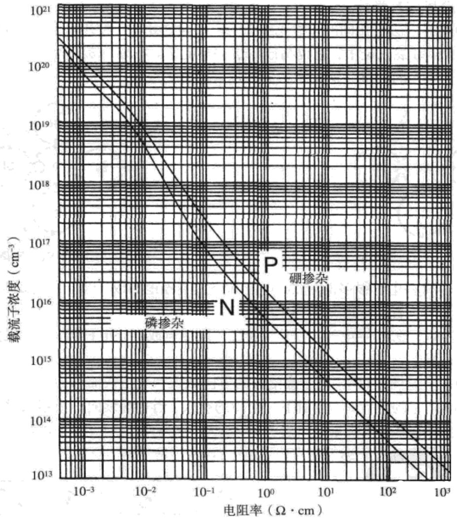
The vertical axis represents carrier concentration, with electrons and holes referred to as carriers. The differing curves for n-type and p-type are due to the varying energy requirements for electron and hole movement. We can see that to achieve a specified resistivity, the doping concentration required for n-type is less than that for p-type.
Only 0.000001% to 0.1% doping is needed to bring the semiconductor into a useful resistivity range, allowing for precise control of resistivity.


Metals conduct electricity solely through the movement of electrons, hence they are always n-type. Semiconductor materials can become either n-type or p-type by doping with specific elements, thus conducting electricity through either electrons or holes. Let’s briefly understand n-type and p-type semiconductors:
N-type Semiconductors
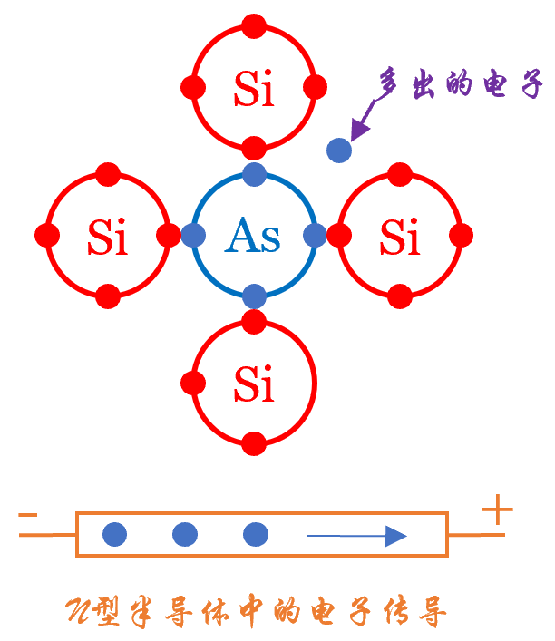
We use arsenic (As) as the doping element in silicon (Si). Assuming each arsenic atom is surrounded by silicon atoms, arsenic has 5 outer electrons, four of which pair with silicon’s electrons, leaving one as a conduction electron. Of course, doping elements can also include phosphorus (P) and antimony (Sb).
P-type Semiconductors
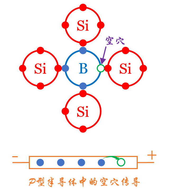
P-type semiconductors are doped with boron (B) from group III of the periodic table, which has only 3 outer electrons. When surrounded by silicon atoms, the three electrons pair with silicon’s electrons, leaving one position without an electron, which is a hole.
In doped semiconductors, electrons and holes continuously form, with electrons being drawn in to fill holes, thus creating a new unfilled position—a new hole.
Today’s content introduced several fundamental concepts, but there is much more involved in semiconductor chip design. I hope you enjoyed it and look forward to continuing this discussion~


Editor: Xiao Huibing