Click the blue text
Follow us

This article introduces the design and implementation of a local control DDS arbitrary waveform generator based on STM32 and FPGA. The project successfully generates adjustable waveforms (sine, triangle, square), frequencies (DC-5MHz), and amplitudes (0.1V-1V) using a high-speed DAC combined with FPGA internal DDS logic, and displays waveform parameters in real-time on an OLED screen. The author shares the entire process from hardware selection, design ideas to code implementation, and discusses the challenges encountered in the project and directions for improvement, providing a highly valuable practical case for electronics enthusiasts and engineers.
Project Introduction


1. Generate adjustable waveforms (sine, triangle, square), adjustable frequencies (DC-), and adjustable amplitudes using the high-speed DAC on the board combined with the internal DDS logic of the FPGA.
2. The frequency range of the generated analog signal is DC-5MHz, with a tuning precision of 1Hz.
3. The amplitude of the generated analog signal is up to 1Vpp, with a tuning range of 0.1V-1V.
4. Display the current waveform shape, frequency, and amplitude on the OLED.
5. Use the onboard rotary encoder and buttons to switch waveforms and adjust parameters.
Design Ideas
1. Hardware and Compilation Environment
This project uses the Lattice ICE40UP5K FPGA and STM32G031 MCU, along with buttons, a rotary encoder, and an OLED display connected to the STM32, and a high-speed DAC connected to the FPGA. The main development environments used are STM32CubeMX, Keil5, and Radiant.
2. Design Block Diagram
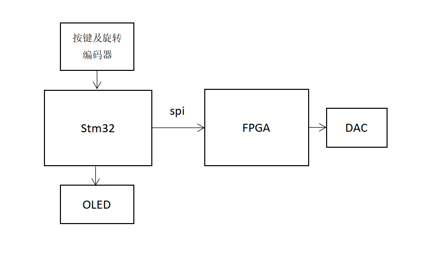
As shown in the figure, the buttons and rotary encoder are connected to the STM32 to input waveform signals, the OLED screen displays information, and the FPGA is connected to the high-speed DAC to generate waveform signals. The STM32 and FPGA are connected via SPI for signal transmission.
Code Sharing
1. Button Input Section
Two buttons and a rotary encoder are used here. Due to the limited resources of buttons, each button is designed to have a single function and be spaced apart. The main inputs needed are the frequency, amplitude, and waveform number, with a frequency range of 0 to 5000000Hz, a precision of 1Hz, an amplitude range of 0 to 1V, and a precision of 0.1V. Button 1 is responsible for switching modes for amplitude, frequency, and waveform, while Button 2 selects each bit of the frequency. The rotary encoder is used for digital input of frequency and amplitude, and to select the waveform. When Button 1 is pressed for the fourth time, the STM32 sends all data to the FPGA and displays the waveform.
Button 1:
if(HAL_GPIO_ReadPin(GPIOA, GPIO_PIN_12)==0){ key1_num++;Button 2:
if(GPIO_Pin == KEY2_Pin)// Second layer button frequency bit selection { delay(10); if(HAL_GPIO_ReadPin(GPIOA, GPIO_PIN_11)==0&&key1_num==2){ num[2]=0; if(wei>=7) wei=0; else wei++; } Rotary Encoder:
if(GPIO_Pin == A_state_Pin) { HAL_TIM_Base_Start_IT(&htim2); if((wei==7&&&num[2]>=5)||num[2]>=9) num[2]=0; if(num[3]>=3) num[3]=0; if(num[1]>=10) num[1]=0; if(flag==1&&&num[key1_num]>=1) { num[key1_num]--; } elseif(flag==2) { num[key1_num]++; } switch(key1_num){ case1:amp=num[1]; break; case2:freq[wei]=num[2]; freq_sum=freq[7]*1000000+freq[6]*100000+freq[5]*10000+freq[4]*1000+freq[3]*100+freq[2]*10+freq[1]; data1=freq[2]*10+freq[1];// Combine frequency data to be sent after pressing Button 2 data2=freq[4]*10+freq[3]; data3=freq[6]*10+freq[5]; data4=freq[7]; break; case3:wave=num[3]; break; default: break; } flag=0; } For debouncing, the two buttons are debounced simply using a custom delay function, while the rotary encoder uses a timer, and the direction of rotation is determined in the timer interrupt. The direction of rotation is primarily judged by the timing of the low-level signals generated at the A and B ends.
void HAL_TIM_PeriodElapsedCallback(TIM_HandleTypeDef *htim){ if(htim==(&htim2)) { if(HAL_GPIO_ReadPin(GPIOB, GPIO_PIN_0)==0) { if(HAL_GPIO_ReadPin(GPIOB, GPIO_PIN_1)==0) flag=1; else flag=2; } HAL_TIM_Base_Stop_IT(&htim2); } } 2. OLED Interface
For the OLED part, I directly used the existing driver code with slight modifications, configuring MOSI and SCK in SPI2 to send data, and software simulating the chip select signal. The interface includes a downward line for better positioning of the button input location.
void show(void){ OLED_ShowString(8,32,(uint8_t *)"WARE:",16,1); OLED_ShowString(8,0,(uint8_t *)"AMP:",16,1); OLED_ShowString(8,16,(uint8_t *)"freq:",16,1); OLED_ShowNum(40,0,amp/10,1,16,1); OLED_ShowString(48,0,(uint8_t *)".",16,1); OLED_ShowNum(54,0,amp%10,1,16,1); OLED_ShowString(104,0,(uint8_t *)"V",16,1); OLED_ShowNum(48,16,freq_sum,7,16,1); OLED_ShowString(104,16,(uint8_t *)"HZ",16,1); switch(wave){ case0:OLED_ShowString(56,32,(uint8_t *)"DC ",16,1);break; case1:OLED_ShowString(56,32,(uint8_t *)"square ",16,1);break; case2:OLED_ShowString(56,32,(uint8_t *)"triangle",16,1);break; case3:OLED_ShowString(56,32,(uint8_t *)"sine ",16,1);break; default:break; } switch(key1_num){ case1:OLED_DrawLine(8,15,31,15,1);break; case2:{OLED_DrawLine(8,31,39,31,1);OLED_DrawLine(8,15,31,15,0);break;} case3:{OLED_DrawLine(8,31,39,31,0);OLED_DrawLine(8,47,39,47,1);break;} default:{OLED_DrawLine(8,15,31,15,0);OLED_DrawLine(8,31,39,31,0);OLED_DrawLine(8,47,39,47,0);break;} } if(key1_num==2){ switch(wei){ case7:{OLED_DrawLine(56,31,63,31,0);OLED_DrawLine(48,31,55,31,1);break;} case6:{OLED_DrawLine(64,31,71,31,0);OLED_DrawLine(56,31,63,31,1);break;} case5:{OLED_DrawLine(72,31,79,31,0);OLED_DrawLine(64,31,71,31,1);break;} case4:{OLED_DrawLine(80,31,87,31,0);OLED_DrawLine(72,31,79,31,1);break;} case3:{OLED_DrawLine(88,31,95,31,0);OLED_DrawLine(80,31,87,31,1);break;} case2:{OLED_DrawLine(96,31,103,31,0);OLED_DrawLine(88,31,95,31,1);break;} case1:{OLED_DrawLine(96,31,103,31,1);break;} default:{OLED_DrawLine(48,31,55,31,0);break;} } } OLED_Refresh();}3. Communication between STM32 and FPGA
For the STM32 part, I also used the principle of SPI communication with the OLED screen, controlling the chip select via software, configuring MOSI and SCK in SPI2 to send data. The waveform information is divided into 6 bytes and sent sequentially. To align, the amplitude and waveform data are each set to one byte, while the frequency data is divided into 4 bytes.
printf("hello world!"); if(key1_num==4)      {                            // Send 6 bits of data at once          spi1_cs_set();// Amplitude data            HAL_SPI_Transmit(&hspi1, &amp, 1, 1000);      spi1_cs_res();
      spi1_cs_set();// Waveform      HAL_SPI_Transmit(&hspi1, &wave, 1, 1000);      spi1_cs_res();                                spi1_cs_set();// Frequency data 1      HAL_SPI_Transmit(&hspi1, &data1, 1, 1000);      spi1_cs_res();                                spi1_cs_set();// Frequency data 2      HAL_SPI_Transmit(&hspi1, &data2, 1, 1000);       spi1_cs_res();                                spi1_cs_set();// Frequency data 3      HAL_SPI_Transmit(&hspi1, &data3, 1, 1000);      spi1_cs_res();                                spi1_cs_set();// Frequency data 4      HAL_SPI_Transmit(&hspi1, &data4, 1, 1000);      spi1_cs_res();                                                                          key1_num=0;
The FPGA part references code from Eetreehttps://www.eetree.cn/wiki/spi_verilog, processing the received data. The SCK rate of the STM32 is adjusted to match the 12M clock frequency on the FPGA. Through testing, the data received by the FPGA is relatively stable when the SPI of the STM32 operates at approximately 1000kBits/s.
module stm_fpga_spi(clk, SCK, MOSI, SSEL,freq,ware, amp,LED1);input clk;input SCK, SSEL, MOSI;
output reg LED1;output reg [7:0] amp;output reg [7:0] ware;output reg [23:0]freq;
// sync SCK to the FPGA clock using a 3-bits shift registerreg [2:0] SCKr;  always @(posedge clk) SCKr <= {SCKr[1:0], SCK};wire SCK_risingedge = (SCKr[2:1]==2'b01);  // now we can detect SCK rising edgeswire SCK_fallingedge = (SCKr[2:1]==2'b10);  // and falling edges
// same thing for SSELreg [2:0] SSELr;  always @(posedge clk) SSELr <= {SSELr[1:0], SSEL};wire SSEL_active = ~SSELr[1];  // SSEL is active lowwire SSEL_startmessage = (SSELr[2:1]==2'b10);  // message starts at falling edgewire SSEL_endmessage = (SSELr[2:1]==2'b01);  // message stops at rising edge
// and for MOSIreg [1:0] MOSIr;  always @(posedge clk) MOSIr <= {MOSIr[0], MOSI};wire MOSI_data = MOSIr[1];
// Receiving part// we handle SPI in 8-bits format, so we need a 3 bits counter to count the bits as they come inreg [2:0] bitcnt;
reg byte_received;  // high when a byte has been receivedreg [7:0] byte_data_received;always @(posedge clk)begin  if(~SSEL_active)    bitcnt <= 3'b000;  else  if(SCK_risingedge)// Sample on rising edge  begin    bitcnt <= bitcnt + 3'b001;
    // implement a shift-left register (since we receive the data MSB first)    byte_data_received <= {byte_data_received[6:0], MOSI_data};  endend
// Indicate that reception is completealways @(posedge clk)   byte_received <= SSEL_active && SCK_risingedge && (bitcnt==3'b111);  // Count the 6 groups of datareg [7:0] count;always @(posedge clk) begin  if(byte_received)begin    if(count>=5)begin       count<=0;                end    else    count<=count+8'h1;  // Count the messages    endend     reg [31:0] freq_temp; reg [7:0]ware_temp; reg [7:0]amp_temp; reg flag;// Divide into six states to receive different dataalways @(posedge clk)     if(byte_received) begin     case(count)       0:amp_temp= byte_data_received;         1:ware_temp= byte_data_received;       2:freq_temp[7:0]= byte_data_received;       3:freq_temp[15:8]= byte_data_received;       4:freq_temp[23:16]= byte_data_received;       5:begin freq_temp[31:24]= byte_data_received;end                                default:begin  ware_temp =0;                         amp_temp  =0;               freq_temp =0;                                           end        endcase end    // When count=5, combine the received dataalways @(posedge clk)     if(byte_received) begin      if(count==5)begin    freq<=freq_temp[7:0]+freq_temp[15:8]*100+freq_temp[23:16]*10000+freq_temp[31:24]*1000000;    ware<=ware_temp;    amp<=amp_temp;  end  end   endmodule
4. DDS Section
This part references materials on DDS from Eetreehttps://www.eetree.cn/wiki/dds_verilog and other resources. First, the clock frequency is increased to 120MHz using a PLL, directly utilizing the IP core provided by Radiant software. A 41-bit phase accumulator is used to achieve a precision of 0.0000546Hz. The frequency data received is multiplied by 18325 to achieve a precision of 1Hz, enabling adjustable frequency.
wire clk_120M;pll_120M u_pll_120( .ref_clk_i (clk), .rst_n_i(rst_n), .outcore_o(clk_120M), .outglobal_o() ); reg [40:0] phase_add; always @(posedge clk_120M or negedge rst_n) begin if(!rst_n) begin phase_add <=0; end else phase_add <= phase_add + freq_input_dds*18325; endImplementation of square and triangle waves:
assign square_data = phase_add[40] ? 10'd1023:10'd0; assign triangle_data=phase_add[40] ? ~phase_add[39:30]:phase_add[39:30]; assign DC=10'h3FF;Implementation of sine waves primarily utilizes a lookup table. I generated waveform information using MATLAB, retaining one-quarter of the waveform data and using symmetry to map the entire waveform.
lookup_tables u_lookup_tables(.phase(phase_add[40:31]),.sin_out(sin_data));assign sin_out = sine_onecycle_amp[9:0];assign sel = phase[9:8];sin_table u_sin_table(address,sine_table_out);
always @(sel or sine_table_out)begin case(sel) 2'b00: begin sine_onecycle_amp = 9'h1ff + sine_table_out[8:0]; address = phase[7:0]; end 2'b01: begin sine_onecycle_amp = 9'h1ff + sine_table_out[8:0]; address = ~phase[7:0]; end 2'b10: begin sine_onecycle_amp = 9'h1ff - sine_table_out[8:0]; address = phase[7:0]; end 2'b11: begin sine_onecycle_amp = 9'h1ff - sine_table_out[8:0]; address = ~ phase[7:0]; end endcaseendResults and Observations
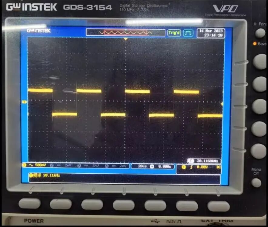
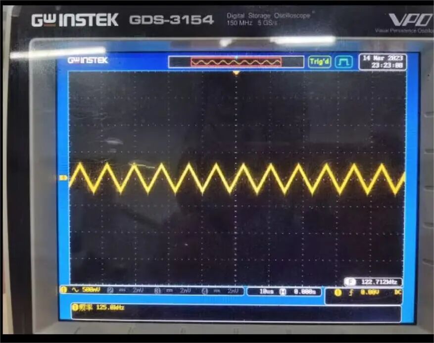
Swipe to see more
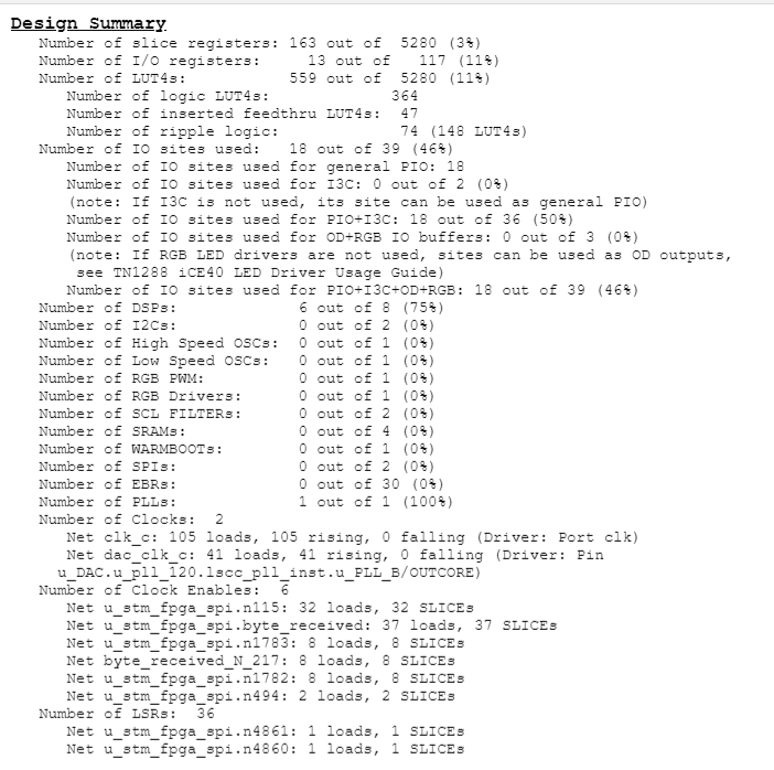
Resource Usage:
Areas for Improvement:
– The method for determining the rotation direction of the rotary encoder is relatively simple and crude, leading to some instability in actual input. Future attempts could explore timer-based encoder modes for decoding.
– The overall input of waveform information requires all information to be input before transmitting the signal to generate the waveform. Future attempts could allow for real-time input of various information.
– The final waveform effect is not particularly good, with some distortion occurring at high frequencies. Some filtering algorithms could be tried to improve precision.
Insights and Reflections
Overall, this project is relatively simple, but many issues arose during the process, and due to my limited skills, many parts of the code were written quite simply, resulting in many imperfections in the final outcome.
Through this activity, I feel that my greatest gain is the improvement of my problem-solving ability, finding relevant information online, and debugging the code step by step to identify where the problem lies and then making modifications. The communication between STM32 and FPGA was the last part I worked on. I initially thought it would be simple, but I unexpectedly got stuck for a long time. I didn’t know whether the problem was on the STM32 side or the FPGA side, and after a lot of debugging with the debug lights and simulation, I gradually narrowed down the range and finally achieved successful communication.
Based on the shortcomings of this project, I will continue to improve and learn more in the future.

Click “Read the original text” to view the project