
Click the blue text to follow us


Introduction

The previous article introduced the physical and chemical properties and crystal structure of silicon carbide materials, which lay a solid foundation for the wide application of silicon carbide materials in industries such as aerospace, electronics, and energy. This article continues to introduce the preparation processes and application scenarios of silicon carbide materials.

Preparation Processes of Silicon Carbide
The preparation processes of silicon carbide materials mainly include the following methods:
Physical Vapor Transport (PVT)
The PVT method is currently the most widely used method in industrial production. Its principle is to use high-purity carbon powder and high-purity silicon powder to sublime into a gas phase at high temperatures, which is then transported to a low-temperature seed crystal for crystallization and growth of silicon carbide crystals. This method has simple equipment, low cost, and easy control of operations, but the crystal growth rate is slow, and it is prone to side reactions and crystallization defects.
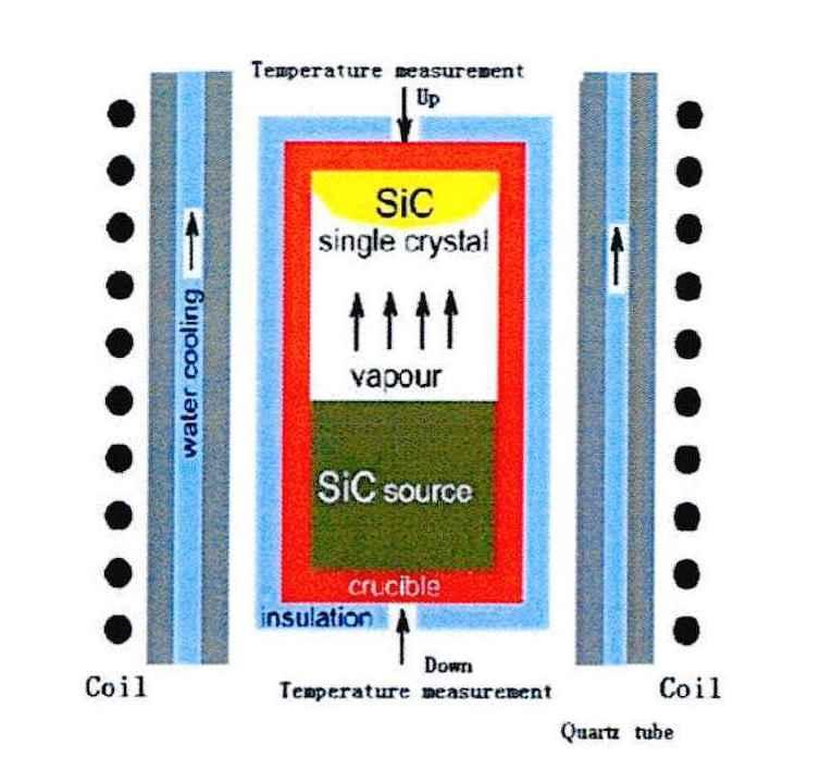
Figure 3: Schematic of SiC Growth by Physical Vapor Transport Method
Chemical Vapor Deposition (CVD)
The CVD method decomposes silicon-containing gases (such as methane, silane) and carbon source gases under high temperature and high pressure conditions to generate silicon carbide thin films deposited on substrates. This method is suitable for producing high-quality silicon carbide thin films, which have high purity and uniformity, but the equipment cost is high, and the process is complex, making it suitable for laboratory and small-scale production.
Liquid Phase Epitaxy (LPE)
The LPE method grows silicon carbide crystals through the dissolution and precipitation principle, utilizing the dissolution-precipitation process at low temperatures. This method can reduce dislocations and defects, improving crystal quality, but the equipment is expensive, the crystal growth rate is slow, and the size is limited, mainly used for laboratory research.
High-Temperature Chemical Vapor Deposition (HT-CVD)
The HT-CVD method combines the advantages of the CVD method, using high-purity gas raw materials, allowing for doping control and crystal form optimization at lower temperatures, resulting in silicon carbide crystals with fewer defects. The reaction equation involved in HT-CVD is:
2SiH4 + C2H4 = 2SiC + 6H2
In this process, the reaction gases are introduced into the reaction chamber using hydrogen or inert helium as the carrier gas, and the exhaust gases produced by the reaction are treated before harmless discharge. However, compared to other methods, the equipment cost is high, and the degree of commercialization is low.
Top Seeded Solution Growth (TSSG)
Figure 4 is a schematic of the TSSG method for growing 4H-SiC single crystals. Unlike the PVT method, the solution method grows SiC crystals at the solid-liquid interface. The TSSG method is mainly suitable for small-size crystal growth at the laboratory scale, growing crystals by depositing silicon carbide particles from the solution onto the seed crystal, but its crystal growth efficiency is low, mainly used for scientific research and small-scale experiments.
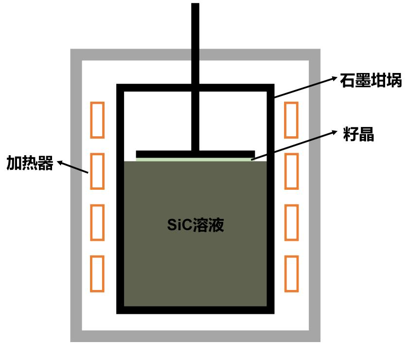
Figure 4: Schematic of TSSG Method for Growing 4H-SiC Single Crystals
Other Methods
These include sol-gel methods, direct synthesis methods, and polymer pyrolysis methods, each with its characteristics, but generally used for specific fields or experimental stages.
In summary, PVT method has become the main method for industrial production of silicon carbide due to its mature technology, low cost, and suitability for large-scale production, while CVD and LPE methods have advantages in thin film preparation and high-quality crystal growth.
Application Scenarios of Silicon Carbide
Typical application scenarios of silicon carbide (SiC) in power electronic devices include the following aspects:
New Energy Vehicles: Silicon carbide power devices are widely used in the main inverters, onboard chargers, and power control units of electric vehicles, significantly improving range, reducing system weight and volume, while enhancing efficiency and reliability.
Photovoltaic and Wind Power Generation: Silicon carbide devices are used in photovoltaic inverters and grid-connected inverters for wind power generation, improving energy conversion efficiency, reducing losses, and supporting distributed generation and energy storage systems.
Rail Transit: Silicon carbide power devices are used in traction converters, auxiliary converters, and other equipment, effectively reducing equipment weight, enhancing power density and efficiency, while meeting lightweight and energy-saving requirements.
Smart Grids: Silicon carbide devices are applied in high-voltage direct current (HVDC) converter valves, flexible HVDC converter valves, AC transmission devices, and HVDC circuit breakers, improving the voltage capacity and reliability of the system.
Industrial Power Supplies and Data Centers: Silicon carbide power devices are used in industrial power supplies, server power supplies, and power management in data centers, helping to reduce energy consumption and improve system performance due to their high efficiency and high power density.
Charging Infrastructure: Silicon carbide devices are applied in charging pile modules, enabling more efficient and compact charging solutions while reducing energy consumption and heat dissipation requirements.
Due to its excellent physical properties, such as high breakdown voltage, high thermal conductivity, and low on-resistance, silicon carbide has a broad application prospect in the field of high voltage, high frequency, and high power power electronics, making it an important direction for future power electronics technology.
Future Outlook
The silicon carbide market is expected to exceed $6 billion by 2025, with a CAGR of 30%. Directions for technological breakthroughs include:
Substrate Size Upgrade: Transitioning from 6 inches to 8 inches, reducing costs by 30%.
Vertical Integration Model: IDM companies (such as Wolfspeed) control the entire chain from substrate to epitaxy to devices.
Emerging Applications: Aerospace nuclear energy (radiation resistance), quantum computing (color center single photon sources).
As a core material of third-generation semiconductors, silicon carbide is driving a revolution in energy conversion efficiency. With the maturation of preparation processes and cost reduction, its irreplaceability in high power, high temperature, and high frequency fields will further highlight.
Data in this article is compiled from IEEE Xplore, Materials Today, Yole Développement industry reports, and technical white papers from companies such as Wolfspeed and Infineon. Key parameters (such as bandgap, thermal conductivity, etc.) reference authoritative studies from the Journal of Applied Physics and Nature Materials.
END