01 Leader: Architect of Domestic Substitution Strategy with a Global Perspective
The technological breakthrough of ZKFC is fundamentally rooted in the “Research-Industry-Capital” three-dimensional strategic system established by its founder and chairman, Dr. Chen Lu. Born in 1977, Chen Lu possesses both a top-tier academic background and international industry experience: he entered the Youth Class of the University of Science and Technology of China at the age of 15, obtained a Ph.D. in Optical Physics from Brown University at the age of 26, and subsequently served as a systems scientist and senior scientist at global semiconductor equipment giants Rudolph Technologies (RTEC) and KLA, deeply involved in the technological iteration of three generations of semiconductor testing equipment, with optical detection algorithm patents he led still widely used in the industry today.
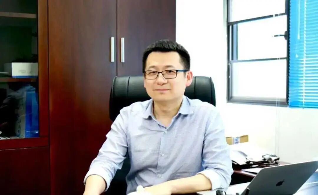
In 2010, responding to the national “Hundred Talents Program,” Chen Lu gave up a million-dollar annual salary abroad to return to China, serving as a researcher and doctoral supervisor at the Institute of Microelectronics of the Chinese Academy of Sciences, leading the establishment of a semiconductor measurement technology laboratory, and undertaking a total of seven national-level projects including the National 863 Program and major scientific and technological special projects, laying the core technological foundation for industrialization. In 2014, Chen Lu and his team moved south to Shenzhen to establish ZKFC, establishing a technological route of “skipping following and directly catching up,” completing the research and development of the first principle prototype in a temporary office area of 200 square meters. As of November 2025, Chen Lu and the core team collectively hold 30.54% of the shares, and the “3+1” strategy (three major core equipment series + one intelligent software ecosystem) they formulated has been fully implemented, leading the company to become the only domestic equipment supplier covering the entire front-end detection process.
02 Core Technology Team: A Collaborative Matrix of Industry, Academia, and Research
1. Core of Technological Breakthrough: Huang Youwei’s Team’s Leapfrog Project
The core technology team led by Huang Youwei, a model worker in Guangdong Province and R&D director, has built a closed-loop system for tackling challenges based on “fundamental research-engineering-industrialization.” When he joined in 2016, Huang Youwei’s team faced KLA’s 30-year technological monopoly in defect detection, innovatively proposing a collaborative optimization plan of “optical system-algorithm-mechanical structure,” decisively skipping the second-generation equipment technology route and directly targeting the fourth-generation high-resolution detection platform. By independently designing a vacuum ultraviolet optical system and developing sub-nanometer-level positioning algorithms, the team completed a leapfrog breakthrough from 90nm to 14nm processes in just three years, with the SPRUCE series of non-patterned wafer defect detection equipment achieving a detection accuracy of 0.3nm, reducing the error compared to international competitors by 0.1 nanometer units, becoming the core supporting equipment for SMIC and Yangtze Memory Technologies’ advanced process production lines at 28nm and below.
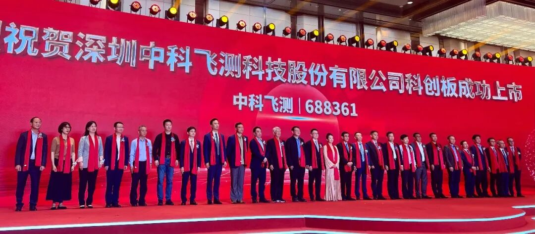
As of November 2025, the technological achievements led by Huang Youwei’s team have achieved three major breakthroughs: first, the 7nm node equipment has completed small batch shipments, with a global market share rising to 18%, ranking second globally; second, the 3DAOI detection equipment developed has improved detection efficiency in the HBM packaging field by 20% compared to international competitors, capturing over 60% of the domestic market share; third, they have led the formulation of three national standards including the “Technical Specifications for Semiconductor Wafer Defect Detection Equipment.” The “project-based + mentorship” talent training system they established has nurtured 23 core technical leaders, including Zhao Kangjun (Ph.D. from Tsinghua University), and the team has received multiple honors such as the “Shenzhen Workers’ Pioneer” and the “Guangdong Province May Day Labor Award.”
2. Talent Structure: A Composite Configuration of “Zhongke System + International Talent”
The core team of the company exhibits characteristics of “high education, high qualifications, and strong collaboration”: there are currently 610 employees, with R&D personnel accounting for 62.3%, including 28 PhDs and 215 master’s degree holders, and over 90% of R&D personnel have more than five years of experience in the semiconductor equipment industry. The team structure forms three major pillars:
①Core Members from the Chinese Academy of Sciences: 12 core members come from the Institute of Microelectronics of the Chinese Academy of Sciences, including three major project leaders, four doctoral supervisors, leading the research and development of foundational optics, precision machinery, and other underlying technologies;
②Senior Experts from International Giants: 18 technical backbones from international leading companies such as KLA and Applied Materials (AMAT) have been recruited, covering key links such as equipment engineering and production line verification;
③Interdisciplinary Young Talents: Top interdisciplinary talents from Tsinghua University, Peking University, and the University of Science and Technology of China have been introduced to build a collaborative system of four major disciplines: “Optical Engineering-Software Algorithms-Automation Control-Materials Science”.
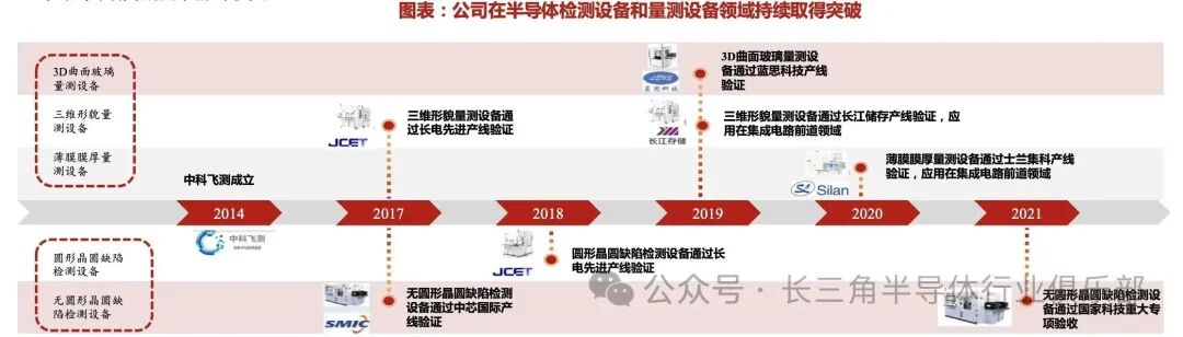
As of November 2025, the team has applied for a total of 687 domestic and international patents, of which 623 have been authorized (158 invention patents), with a 100% self-controllable rate of core technologies, forming a patent matrix covering the entire semiconductor manufacturing process.
03 Team Governance and Culture: Institutional Guarantee for Technological Innovation
1. Strategic Orientation: Anchoring Core Pain Points in the Industry Chain
The team has always focused on the core mission of “solving bottleneck problems,” concentrating on key areas where the domestic substitution rate of semiconductor testing equipment is less than 10%, and has formulated a “two-step” strategy: the first step (2014-2025) is to achieve domestic substitution of mature process (28nm) equipment, and the second step (2025-2030) is to tackle core equipment for advanced processes (3nm and below). By 2025, the 28nm lithography machine supporting detection equipment led by the team will achieve exclusive domestic supply, helping to increase the domestic substitution rate of semiconductor testing equipment from less than 5% to 25%.
2. R&D System: High-Intensity Investment and Industry-Academia-Research Collaboration
A three-tier R&D system has been established: “Company R&D Center + Joint Laboratory with the Chinese Academy of Sciences + University Internship Base”: from 2022 to the first three quarters of 2025, a total of 1.28 billion yuan has been invested in R&D, with the total R&D investment expected to reach 720 million yuan in 2025, maintaining a revenue ratio of over 28%; a “Joint Laboratory for Semiconductor Measurement Technology” has been co-established with the Institute of Microelectronics of the Chinese Academy of Sciences, undertaking two national major scientific and technological special projects; and postdoctoral workstations have been set up in cooperation with Tsinghua University, Shanghai Jiao Tong University, and other universities, training 46 professionals in semiconductor equipment.
3. Incentive Mechanism: Core Talents Grow Together with the Company
A diversified incentive system of “equity + project bonuses + technology achievement transformation rewards” has been implemented: the shareholding ratio of core technical personnel has reached 15.3%, with an annual technology innovation reward fund of 50 million yuan established, providing up to 5 million yuan in special rewards for teams achieving key technological breakthroughs. As of 2025, eight task teams have received excess rewards through technology achievement transformation, forming a virtuous cycle of “R&D-transformation-incentive-re-R&D.”
04 Strategic Implementation and Industry Contribution: From Technological Breakthroughs to Industrial Empowerment
1. Key Project Progress
①Second Headquarters in Zhangjiang, Shanghai: Construction will start in May 2025, with an investment of over 1 billion yuan to create a 130,000 square meter R&D and industrialization base. The main structure has been completed, and it is expected to officially start production in the second quarter of 2026, with an annual production capacity of 300 advanced process detection equipment, reducing the delivery cycle from 6-8 months to 3-4 months;
②EUV Detection Technology Layout: The team has completed the development of a prototype EUV detection device based on HHG (High Harmonic Generation) technology with a wavelength of 13.5nm, suitable for defect detection in processes below 5nm, with a detection speed improved by over 100 times compared to traditional electron beam devices, and a resolution of 0.1nm, expected to enter the customer verification stage in 2026;
③Overseas Market Expansion: Offices have been established in Singapore and Malaysia, and cooperation memorandums have been signed with two wafer fabs in Southeast Asia, with the overseas revenue ratio expected to increase to 4.8% in 2025 and break through 15% by 2027.
2. Industry Influence
①Technical Standards: Leading or participating in the formulation of 8 semiconductor testing equipment industry standards, including 3 national standards and 5 industry standards;
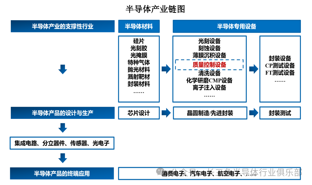
②Industry Chain Collaboration: Jointly established the “Semiconductor Testing Equipment Domestic Substitution Alliance” with 23 core component suppliers in China, promoting the self-sufficiency rate of key components such as vacuum ultraviolet light sources and high-precision sensors from 60% to 68%;
③Market Position: In the third quarter of 2025, revenue reached 2.14 billion yuan, a year-on-year increase of 120%, with a domestic market share of 25%. The core product, the DRAGONBLOOD series of lithography measurement equipment, ranked second in global market share, becoming the only Chinese semiconductor testing equipment brand to enter the global top two.
05 Future Layout: Building a Talent Ecosystem with Global Competitiveness
The team will continue to focus on three major directions: “technological leadership + talent aggregation + ecological collaboration”: at the technical level, accelerating the R&D of detection equipment for processes of 3nm and below, aiming for commercialization of EUV supporting detection equipment by 2027; at the talent level, planning to introduce 10 top overseas experts in the next three years and train 50 doctoral-level technical talents, increasing the proportion of R&D personnel to over 65%; at the ecological level, deepening collaborative R&D with domestic lithography machine companies such as Shanghai Microelectronics, aiming for a self-sufficiency rate of core components to reach 85% by 2028, ultimately achieving a strategic leap from “domestic substitution” to “global leadership.”
*Disclaimer:
1. The content published on this WeChat public platform is sourced from the internet. It is for informational purposes only and does not represent the views and positions of this platform. If there are any copyright/content authenticity issues, please contact this public account, and we will delete the content promptly.
2. The articles marked as original in this account involve companies and industries that are the author’s personal views or AI searches, and should not be used as investment references. Industry insiders and outsiders are welcome to discuss rationally.
3. Some images in this account’s articles are searched from the internet, and if there is any infringement, please contact us for deletion.
END
We sincerely invite you to join the Wu Luo Yangtze River Delta Semiconductor Club group chat
Joining method/remarks: Company name, name, position, phone
Please scan the QR code to join the group
Welcome colleagues to join the group for communication!