01Introduction
This academic sharing is based on the research work published by Enrique Cantó-Navarro and Mariano López-García in IEEE TRANSACTIONS ON DEPENDABLE AND SECURE COMPUTING in 2025.
Paper Title:AXI Hardware Accelerator for McEliece on FPGA Embedded Systems
Authors:Enrique Cantó-Navarro, Mariano López-García
Source:《IEEE TRANSACTIONS ON DEPENDABLE AND SECURE COMPUTING》,DOI:10.1109/TDSC.2024.3445181
Value Rating:
Method Innovation ★★★★☆
Engineering Value ★★★★☆
Theoretical Depth ★★★☆☆
Main Content:
This article proposes a McEliece hardware accelerator that connects to the AXI infrastructure, achieving runtime programmability through innovative architectural design and configurable parameters, effectively enhancing computational performance and optimizing resource utilization in FPGA embedded systems, suitable for various security-sensitive applications.
Further Reading:
1. Pioneering Literature: Kuo, YM; Garcia-Herrero, F; Maestro, JA, “RISC-V Galois Field ISA Extension for Non-Binary Error-Correction Codes and Classical and Post-Quantum Cryptography” IEEE TRANSACTIONS ON COMPUTERS, 2023, 09/TC.2022.3174587
2. Related Literature: Post-Quantum Biometric Authentication Based on Homomorphic Encryption and Classic McEliece rjona, R; López-González, P; Baturone. Post-Quantum Biometric Authentication Based on Homomorphic Encryption and Classic McEliece. APPLIED SCIENCES-BASEL, 2023 10.3390/app13020757
This article belongs to the field of cryptographic hardware acceleration, primarily addresses the efficient implementation of the McEliece algorithm in FPGA embedded systems and tackles challenges such as poor adaptability of traditional hardware implementations and insufficient external connectivity. Based on specific application instruction processor architecture design concepts, it proposes an AXI runtime programmable McEliece hardware accelerator. This accelerator includes components such as polynomial units and vector cores, along with a set of configurable parameters to achieve different functionalities. The main contributions of this paper include: 1. Providing runtime programmability and connectivity to external memory, breaking previous limitations, suitable for various security-sensitive applications, not limited to key encapsulation mechanisms. 2. Achieving a flexible trade-off between security level, area, and performance through configurable parameters, adaptable to different FPGA devices. 3. Effectively utilizing hardware resources, achieving significant performance improvements on both low-cost and high-end FPGAs, and supporting higher security parameters, surpassing previous related cryptographic processors. The paper demonstrates the effectiveness of the accelerator through experiments and theoretical analysis on different FPGA platforms.
02Literature Background
In the current era of rapid development of quantum computing, traditional public key cryptographic algorithms face severe challenges, which constitutes the core background of this research. Specifically, its literature background covers the following key aspects:
1. Quantum computing threatens the security of traditional public key cryptographic algorithms: The emergence of quantum computing algorithms poses potential threats to widely used public key (PK) algorithms, such as RSA and those based on Elliptic Curve Cryptography (ECC). This has prompted researchers to focus on post-quantum (PQ) algorithms that are resistant to quantum computers, providing important contemporary context and research motivation for this study based on the McEliece algorithm.
2. Development and classification of post-quantum cryptographic algorithms: Post-quantum algorithms applied to PK cryptography are mainly divided into five categories: code-based, lattice-based, hash-based, multivariate quadratic equations, and elliptic curve isogeny. Code-based cryptography, represented by the McEliece algorithm and its variants, is well understood and relatively mature in systematic development, occupying an important position in the research of many post-quantum cryptographic algorithms, forming a significant foundation for this paper’s focus on the McEliece algorithm.
3. Evolution and application of the McEliece algorithm: Classic McEliece (CMcE), as a key encapsulation mechanism candidate for NIST standards, is based on the Niederreiter algorithm, replacing Reed-Solomon (RS) codes with binary Goppa codes as the error correction mechanism, and is considered to have post-quantum security. Its characteristics in key generation, encryption, and decryption have sparked extensive research on hardware implementations, providing a direct algorithmic basis and research direction for this study.
4. Current status and limitations of McEliece algorithm hardware implementations:: Previous hardware implementations of the McEliece algorithm have been limited, while there are relatively more hardware implementations of CMcE, but most have limitations. Most systems are built on independent cryptographic processors based on specific fixed computation blocks, with poor connectivity to embedded microprocessors and external memory, and experimental results are often based on theoretical execution times, without considering many factors in practical applications, such as real-time loading of keys and data, and hardware resources used for external bus interfaces. These limitations provide a clear research entry point for proposing new hardware accelerator designs.
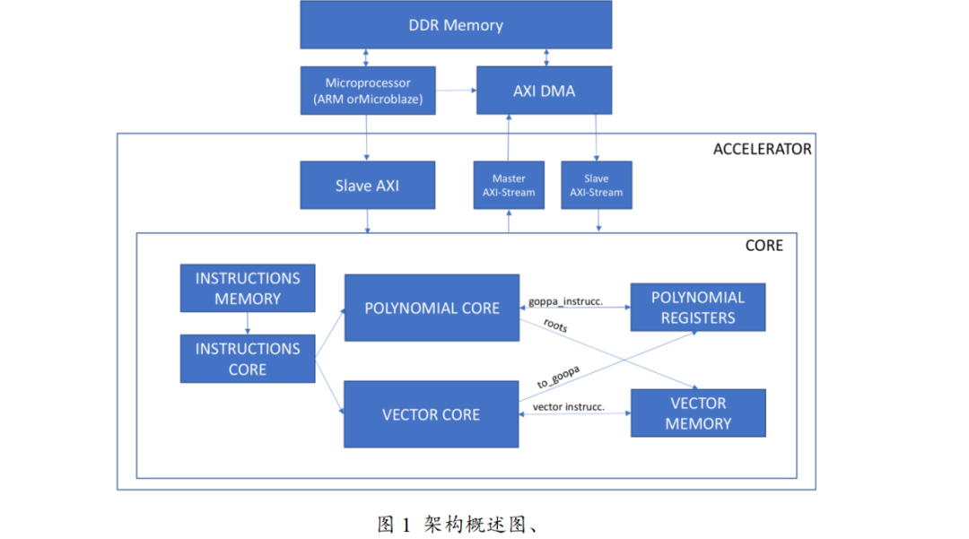
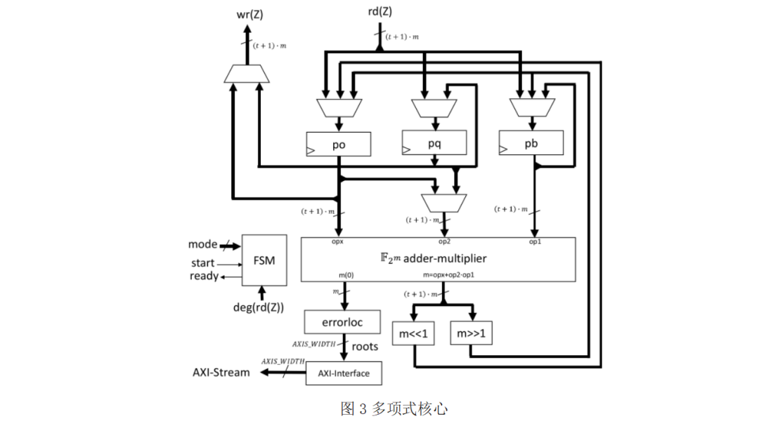
The architecture of the McEliece hardware accelerator designed here is built around a specific application instruction processor, with multiple key components working together to achieve efficient post-quantum cryptographic processing, mainly including the following parts:
Core Processing Unit: Includes polynomial F2m[Z] units and vector cores. The polynomial unit is responsible for operations related to polynomials, with its internal polynomial register file capable of storing polynomial operands and results, reducing access to external DDR memory. The vector core focuses on binary vector operations, with instructions that can compute vector data read from external memory and write back results.
Instruction and Memory System: Instructions are stored in internal memory and can be programmed at runtime, allowing for flexible changes to operations sent to the core. The polynomial register file and vector memory provide data storage support for the two cores, with the polynomial register file consisting of a configurable number of registers, and the maximum bit width of vector memory also configurable, implemented using dual-port BRAM for easy interaction with external data.
Interface Module: Connected to external RAM via AXI-Stream interface and AXI-DMA, achieving efficient data transfer. The Slave-AXI interface is used for the microprocessor to control the accelerator, including setting AXI-Stream interface parameters, starting computation tasks, and obtaining core status.
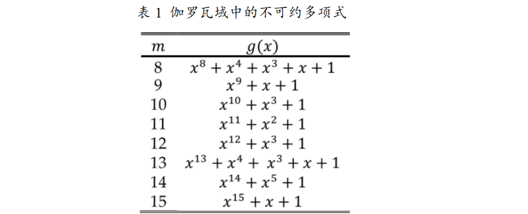
Parameter Configuration Mechanism: Features rich configurable parameters, such as security parameters (nMAX, m, t) determined during synthesis, affecting the polynomial core and its registers; runtime programmable code lengths adaptable to different application needs. Additionally, parameters such as instruction memory depth (NUM_INST), number of polynomial registers (NUM_REGS), AXI-Stream interface width (AXIS_WIDTH), and the parallelism factor of the Galois-Field F2m adder-multiplier (GF2MULT_FACTOR) allow for flexible trade-offs between area and performance, enabling the accelerator to adapt to different FPGA devices.
03Research Methodology
In the overall architecture design, the accelerator connects to external RAM via AXI-Stream interface and AXI-DMA, achieving efficient data transfer, while utilizing the Slave-AXI interface for microprocessor control of the accelerator, including interface parameter settings, task initiation, and status retrieval. This design breaks the limitations of traditional independent cryptographic processors, enhancing the system’s interaction capabilities with the external environment.
In terms of core components, two key modules, the polynomial F2m unit and the vector core, have been constructed. In the polynomial unit, the core computational logic is built around a parallel F2m adder-multiplier, with basic operations based on finite field F2m operations. For example, in the finite field F2m, addition is equivalent to bitwise XOR, for two elements a, b ∈ F2m, it can be represented as c = a ⊕ b; multiplication is based on an irreducible polynomial p(Z), let a(Z), b(Z) ∈ F2m[Z], the multiplication operation c(Z) = a(Z) ⋅ b(Z) mod p(Z). The register file within the polynomial unit can store operands and results, significantly reducing access to external DDR memory and improving computational efficiency. The vector core focuses on binary vector operations, with instructions that can compute vector data read from external memory and write back results. The two work collaboratively, providing strong computational support for cryptographic processing.
The design of the instruction and memory system is quite ingenious. Instructions are stored in internal memory, supporting runtime programming, allowing for flexible adjustments to core operations. For example, the operation flow of polynomial core instructions is based on finite state machine control, with different instruction execution steps being similar, achieving diverse operations through configurable parameters. The polynomial register file and vector memory provide data storage for the two cores, with the former having a configurable number of registers, and the latter implemented using dual-port BRAM, optimizing data interaction processes.
The parameter configuration mechanism is a highlight of this design. Security parameters are determined during synthesis, affecting the architecture of the polynomial core. Parameters such as code length n, and the dimensions of the parity-check matrix H, determine the algorithm’s security and computational complexity. The runtime programmable code length n (n ≤ nMAX) adapts to different application needs. Additionally, parameters such as instruction memory depth (NUM_INST), number of registers (NUM_REGS), AXI-Stream interface width (AXIS_WIDTH), and the parallelism factor of the Galois-Field F2m adder-multiplier (GF2MULT_FACTOR) achieve flexible trade-offs between area and performance. For example, by adjusting the parallelism factor GF2MULT_FACTOR, the degree of parallelism in finite field multiplication can be altered, finding a balance between hardware resource consumption and computation speed, enabling the accelerator to adapt to different performance FPGA devices.
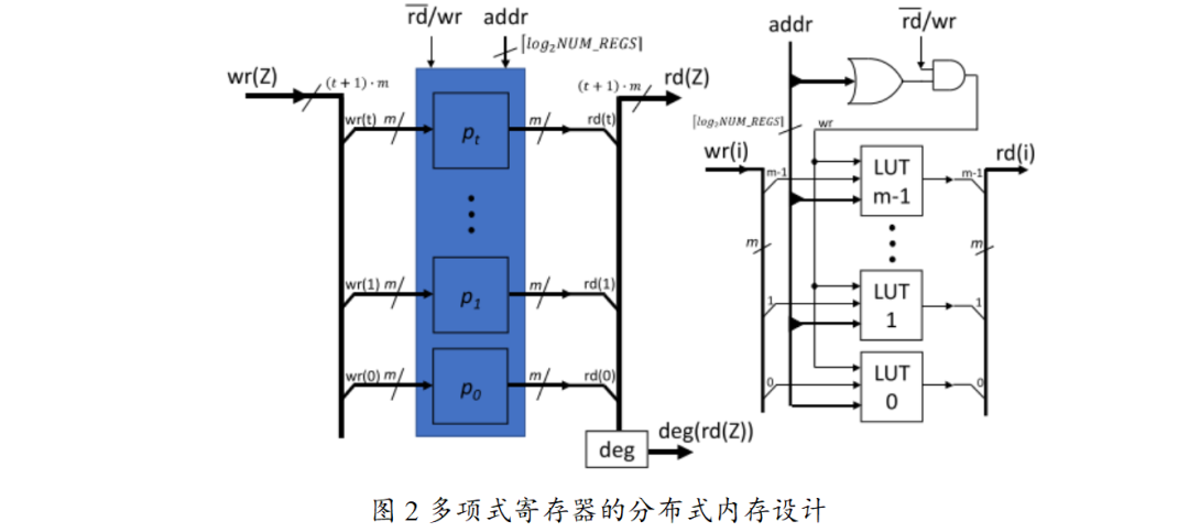
Design Purpose: To reduce the frequent access to external DDR memory during polynomial operations, lower data read latency, and enhance overall computational efficiency, this design employs distributed memory to store polynomial operands and results, allowing the polynomial unit to quickly access and store data, avoiding performance bottlenecks caused by external memory access.
Specific Structure: The polynomial register file consists of a configurable number (NUM_REGS) of registers, and it is recommended to set this to a power of 2 to optimize memory usage and data processing efficiency. These registers can store polynomial coefficients and intermediate results, and also include special-purpose registers for storing irreducible polynomials, polynomial lengths, and other key information, facilitating quick access during operations.
Working Principle: During polynomial operations, data is read from and written to the register file directly, without frequent access to external memory. For example, when performing polynomial multiplication in the finite field F2m, c(Z) = a(Z) ⋅ b(Z) mod p(Z), the coefficients of a(Z) and b(Z) can be quickly retrieved from the registers, and the result c(Z) can also be promptly stored in the registers, significantly shortening data processing time.
Through the AXI-Stream interface connected to AXI-DMA, data transfer between the register file and external RAM can be achieved, ensuring efficient interaction of data when initial data needs to be loaded or final results need to be saved; at the same time, the microprocessor can configure and control the register file through the Slave-AXI interface, such as setting the number of registers, initializing special-purpose registers, etc., ensuring that the entire polynomial operation process proceeds as planned.
The distributed memory design of the polynomial registers is an important component of this accelerator to enhance performance and flexibility, aiming to reduce external memory access, improve computational efficiency, and adapt to different configuration needs. To reduce the frequent access to external DDR memory during polynomial operations, lower data read latency, and enhance overall computational efficiency, this design employs distributed memory to store polynomial operands and results, allowing the polynomial unit to quickly access and store data, avoiding performance bottlenecks caused by external memory access. The polynomial register file consists of a configurable number (NUM_REGS) of registers, and it is recommended to set this to a power of 2 to optimize memory usage and data processing efficiency. These registers can store polynomial coefficients and intermediate results, and also include special-purpose registers for storing irreducible polynomials, polynomial lengths, and other key information, facilitating quick access during operations. During polynomial operations, data is read from and written to the register file directly, without frequent access to external memory. For example, when performing polynomial multiplication in the finite field F2m, c(Z) = a(Z) ⋅ b(Z) mod p(Z), the coefficients of a(Z) and b(Z) can be quickly retrieved from the registers, and the result c(Z) can also be promptly stored in the registers, significantly shortening data processing time. This design connects through the AXI-Stream interface to AXI-DMA, enabling data transfer between the register file and external RAM, ensuring efficient interaction of data when initial data needs to be loaded or final results need to be saved; at the same time, the microprocessor can configure and control the register file through the Slave-AXI interface, such as setting the number of registers, initializing special-purpose registers, etc., ensuring that the entire polynomial operation process proceeds as planned.
The polynomial core is a key component of this hardware accelerator, playing an important role in enhancing the performance and flexibility of the accelerator. Its core objective is to reduce external memory access, improve computational efficiency, and adapt to different configuration needs.
Structurally, the polynomial core is built around a parallel F2m adder-multiplier, with basic operations based on finite field F2m operations. The polynomial register file consists of a configurable number (NUM_REGS, recommended to be set to a power of 2) of registers, which can store polynomial coefficients and intermediate results, and also include special-purpose registers for storing irreducible polynomials, polynomial lengths, and other key information, facilitating quick access during operations.
During operations, data is read from and written to the polynomial register file directly, without frequent access to external DDR memory, greatly shortening data processing time. For example, in polynomial multiplication in the finite field F2m, c(Z) = a(Z) ⋅ b(Z) mod p(Z), the coefficients of a(Z) and b(Z) can be quickly retrieved from the registers, and the result c(Z) can also be promptly stored in the registers. In terms of interaction with other components, the polynomial core connects to external RAM via AXI-Stream interface and AXI-DMA, enabling data transfer for loading initial data or saving final results. At the same time, the microprocessor can configure and control the polynomial core’s register file through the Slave-AXI interface, such as setting the number of registers, initializing special-purpose registers, etc., ensuring that the entire polynomial operation process proceeds as planned.
04Experimental Validation
The McE accelerator is implemented in two different embedded systems: on a low-cost FPGA and on a high-end MPSoC prototype board. The first system is based on a soft-core MicroBlaze processor on an Artix-7A50T device, connected to 256 MB DDR3 memory. The high-end Zynq UltraScale+ XCZU9EG device contains a quad-core embedded 64-bit ARM-A53 processor, connected to 4GB DDR4 memory.
The hardware execution time (Hw) of the accelerator includes programming of the DMA and access to keys, as well as data from external RAM. The software execution time (Sw) is reported as constant-time C code, compiled with maximum optimization for the target microprocessor. The MicroBlaze is configured in 32-bit mode, with all settings for maximum performance, such as enabling cache, barrel shifters, hardware multipliers, and dividers.
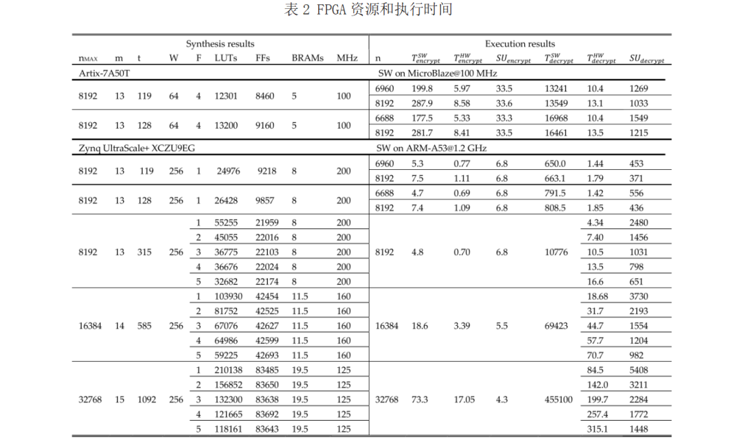
This table presents the synthesized resources of the accelerator on FPGA (LUT, FF, BRAM) and the selected clock frequency (MHz), as well as the execution times (ms) for encryption and decryption on both Sw and Hw, along with the achieved speedup (SU). Security parameters are chosen to the highest level defined on CMcE (m = 13, t = 119, 128, n = 6960, 6688, 8192). Since n can be changed at runtime, ensuring n ≤ nMAX, the synthesized parameter nMAX is fixed at its maximum valid value (2m). For the low-cost Artix-7A50T, the parameters GF2MULT_FACTOR (F=4) and AXIS_WIDTH (W=64) are chosen to fit the available resources, as they share with the embedded soft-core microprocessor and peripherals. In the high-end Zynq UltraScale+ XCZU9EG, the larger available FPGA resources allow for the selection of performance parameters for faster implementations. W=256 is chosen to enhance the speed of access to external memory, and F=1 is chosen to achieve fully parallel F2m adders and multipliers. The security parameters provided by the McE processor are significantly lower than those proposed by the accelerator, making them incomparable. The number of hardware resources on Artix-7 is very low compared to the CMcE processor, ranging from 12301 to 13200 LUTs, from 8460 to 9160 FFs, with only 5 BRAMs. This fact can be explained as the CMcE crypto processor is built from a set of larger computational circuits, each designed for specific stages, with keys and data stored internally in BRAM. In contrast, in the proposed McE accelerator, the computational circuits are reused across multiple stages and retrieve keys from external memory.
However, it is important to note that this comparison is unfair, as the CMcE processor is specifically designed for key encapsulation mechanisms. These encryption processors include key generation circuits, which operate at a much higher frequency compared to the encryption-decryption operations in McE. The execution time using the accelerator varies from 5.33 ms to 8.58 ms for encryption, and from 10.4 ms to 13.5 ms for decryption, operating at a frequency of 100 MHz. When running MicroBlaze at the same clock frequency, the encryption speedup is approximately x33.5, while the decryption speedup ranges from x1033 to x1549. This difference arises because the encryption time is dominated by the matrix-vector multiplication instruction, which is limited by the time taken to read the public key from external memory. However, during decryption, not only are three matrix-vector multiplications executed, but polynomial instructions are also executed. Polynomial instructions are significantly accelerated because the register file is used to read operands and store results, executing computations of the parallel F2m adder.
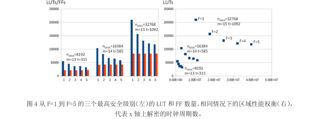
Further increasing F does not significantly reduce the number of LUTs, but the decryption time increases significantly, as shown in the figure. For higher security parameters, changing F=1 to F=2 can reduce the number of LUTs by 25%, but increases the decryption time by 68%. Changing F=4 to F=5 only reduces the LUTs by 3%, while increasing the decryption time by 23%. Finally, from F=1 to F=5, the LUTs decrease by 44%, while the decryption time increases by 273%. However, as the experimental results show, the acceleration is very significant, ranging from x5401 to x1446, and similar behavior can be observed in other reported cases.
Conclusion
The article proposes an AXI runtime programmable McE accelerator that provides a set of configurable parameters. The goal is to offer a flexible accelerator for embedded systems that can adapt to various applications requiring constant-time McE encryption-decryption. Depending on the security parameters required by the application, performance parameters can be selected to achieve optimal area-performance trade-offs in the implementation. To better control FPGA resources and achieve the required clock cycles, this accelerator is designed using HDL language. It provides a set of application-specific instructions for operations with binary vectors, matrices, and Goppa codes, offering AXI connectivity with embedded microprocessors. Keys and instruction memory can be programmed at runtime by this microprocessor, enhancing its flexibility. Experimental results indicate that this accelerator can achieve the highest security parameters of CMcE on both low-cost and high-end FPGAs, achieving decryption speedups of x1549 and x556, respectively.
Such security parameters can significantly improve levels that previous related cryptographic processors could not reach. In larger test cases, the accelerator provides decryption speedups ranging from x5408 to x1448, while using 210138 to 118161 LUTs, depending on the selected trade-offs. The main limitation of the proposed accelerator is the lack of support for key generation. Computing the transpose inverse matrix requires additional circuits and large internal memory, exceeding the resources of low-cost devices. Furthermore, key generation is heavily utilized in KEM (Classic McEliece), but not extensively used in PK encryption-decryption (McEliece). Therefore, providing hardware advantages for key generation instructions in McEliece offers limited benefits and is not suitable for low-cost devices.
(Master’s Year 2: Zhang Zheng)

Changchun University of Technology
Laboratory of Safety and Reliability of Complex Systems
END
 END
END z
z