In the contemporary information technology system, embedded system interfaces serve as the core infrastructure for data exchange, forming the neural hub for device interconnection. Based on standardized communication protocols and interface specifications, the technical architecture enables efficient data exchange and intelligent collaborative operations among heterogeneous devices. This article selects the Analog-to-Digital Converter (ADC) interface as a technical analysis entry point, systematically explaining its working mechanism, performance characteristics, and important parameters, thereby constructing a comprehensive cognitive framework for interface technology for embedded learners and enthusiasts.
1. Basic Concepts
The full name of ADC is Analog-to-Digital Converter, which is an electronic device or module that converts continuous analog signals into discrete digital signals. Embedded systems mostly rely on digital signals for processing, and the ADC converts analog signals into digital signals that can be understood by controllers, enabling devices to monitor, process, and control external physical phenomena.
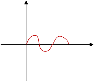
The analog signals collected by the ADC are usually voltage signals. Other types of analog signals, such as temperature, humidity, pressure, light intensity, and current, can be converted into voltage signals through conversion circuits before being collected and converted by the ADC. The waveform of the transmission signal before conversion is shown in the figure below:
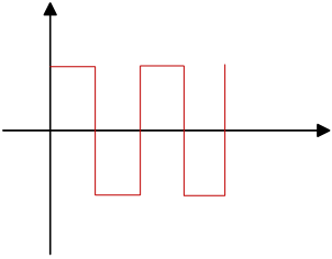
Digital signals are represented by a series of discrete numbers and can only take a limited number of values, generally represented in binary code 0/1. The waveform of the transmission signal after conversion is shown in the figure below:
Compared to the continuous variation of analog signals, the interference of digital signals has a smaller impact on signal quality, allowing for better resistance to external interference during transmission and processing. The ADC converts analog signals into digital signals, enabling precise quantization of signals, allowing complex calculations, control, and analysis to be accomplished through digital means.
2. Working Principle
The ADC completes the conversion from analog signals to digital signals, which mainly includes several key steps: sampling and holding, quantization, and encoding:
(1) Sampling and Holding
The sampling process is performed by the sample-and-hold circuit, which discretizes the continuous analog signal at specific time intervals. This circuit captures the analog signal at a certain sampling frequency, fixing the snapshot (i.e., sampling value) of the analog signal as the voltage value at a specific time point, thereby maintaining the instantaneous level of the signal stable for subsequent quantization and encoding processing.
(2) Quantization
The sampled analog signal is sent to the quantizer of the ADC, which converts the continuously varying analog signal into discrete digital levels. This process is known as quantization. Quantization maps the sampling values to digital levels, approximating each sampling value to the nearest discrete level. This process inevitably produces quantization errors, but it allows the analog signal to be read and processed by the system.
(3) Encoding
After quantization, the encoder converts the discrete quantized values into corresponding binary codes, enabling efficient transmission, processing, and storage of digital signals within the device. Encoding is a critical step in the digitization of analog signals, transforming the quantized values into digital format, ensuring that the signals can be effectively processed within the system.
3. Important Parameters
The performance and accuracy of the ADC are influenced by several important parameters. Here are some key parameters:
(1) Resolution
The resolution of the ADC refers to its ability to distinguish the smallest signal that can be quantized, determining the quantization accuracy. The higher the resolution, the smaller the quantization error and the higher the accuracy. Resolution indicates the number of discrete levels, typically expressed in bits. For example, a 12-bit ADC can represent 2^12 = 4096 levels. When the conversion voltage range is 0~3.3V, the converter divides the range from 0V to 3.3V into 4096 parts.
(2) Sampling Rate
The sampling rate is the number of samples taken by the ADC per second. To ensure the correct completion of the conversion, the sampling rate must generally be less than or equal to the conversion rate, meaning the sampling time must be greater than or equal to the conversion time.
(3) Conversion Time
The conversion time refers to the time required from the start of sampling the analog signal to the completion of digital conversion and output of the digital result by the ADC. Conversion time is an important parameter of ADC performance, especially in high-speed data acquisition systems, where the length of conversion time directly affects the system’s real-time response capability.
(4) Range
The range is the voltage range of the analog signals that the ADC can accept and effectively convert. The actual signal voltage range in application should match this range; exceeding it may lead to saturation or distortion.
This concludes our introduction to ADCs. We hope the above content provides actionable design ideas for embedded development learners and enthusiasts. If you encounter related challenges in your project practice, feel free to message us for further discussion.