Abstract
A research team from Fudan University, East China Normal University, and the Shanghai Institute of Technical Physics, Chinese Academy of Sciences, has designed and fabricated a novel avalanche photodiode (APD) based on a graphene/indium selenide (InSe)/chromium (Cr) asymmetric Schottky junction. This device innovatively realizes the phenomenon of “bidirectional Geiger mode avalanche,” which can occur under both forward and reverse bias, achieving avalanche multiplication. Notably, it achieves a multiplication gain of up to 6.3×10⁷ at a breakdown voltage as low as 1.4 V, which is close to the bandgap threshold limit of InSe material. Thanks to the unique device structure and the excellent properties of InSe material, this APD operates at room temperature with a dark current below 620 fA and can detect weak light signals at approximately 35 photon levels, providing a new strategy for developing efficient, low-power next-generation avalanche optoelectronic devices. The related results were published in Nature Communications.
Research Background
Avalanche photodiodes (APDs) are core devices for detecting weak light signals through the internal carrier avalanche multiplication effect, playing an indispensable role in cutting-edge fields such as optical communication, quantum cryptography, and lidar. However, traditional APDs, such as common silicon-based and InGaAs-based devices, often have inherent defects: they require tens of volts or even higher breakdown voltages to achieve effective signal gain, while defect states introduced during the manufacturing process often lead to higher dark currents, which not only increase system power consumption but also weaken the detection advantages of APDs. In recent years, two-dimensional (2D) layered materials represented by InSe have provided a promising solution for developing low-voltage, high-gain novel APDs due to their unique quantum confinement effects, efficient carrier multiplication, and the ability to form high-quality interfaces with electrodes.
Research Content
The core innovation of this research lies in the clever design of an asymmetric “back-to-back” Schottky junction structure, namely graphene/InSe/Cr. By utilizing the different work functions formed when graphene and chromium metal contact InSe, the researchers constructed two highly different Schottky barriers at both ends of the device, where the graphene/InSe interface barrier is lower (approximately 0.18 eV), while the Cr/InSe interface barrier is higher (approximately 0.54 eV). This asymmetric design successfully spatially separates the “injection region” and “multiplication region” of the carriers. When a forward bias is applied, carriers can easily inject from the low barrier graphene end and then be accelerated in the strong electric field and wider multiplication region formed at the high barrier chromium electrode end, efficiently triggering multiple collision ionizations to achieve avalanche multiplication. Conversely, when a reverse bias is applied, carriers must overcome a higher injection barrier, and the multiplication region is narrower, thus requiring a higher voltage to achieve avalanche, resulting in lower gain. It is this structural asymmetry that leads to the unique “bidirectional” but asymmetric Geiger mode avalanche phenomenon, allowing the device to achieve extremely high gain at very low voltage under forward bias. Additionally, the study found that InSe material has an extremely low critical electric field (11.5 kV/cm) and a special positive temperature coefficient of ionization rate, further promoting the avalanche effect at low voltages.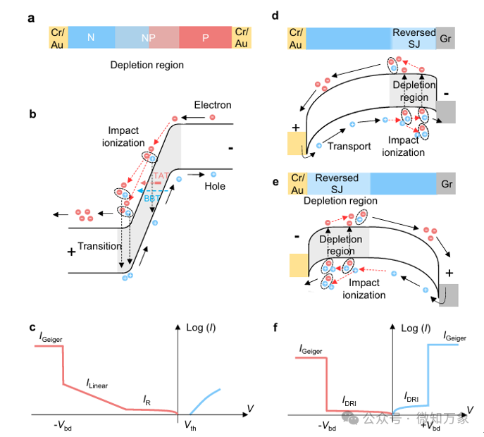
Figure 1 Energy band diagram and transport characteristics of PN junction and two-dimensional SJAPD.
Based on the unique design mentioned above, the Graphene/InSe/Cr avalanche photodiode (GISC-SJ APD) exhibits world-class performance. At room temperature, the device’s breakdown voltage can be as low as 1.4 V, which is very close to the theoretical limit corresponding to the 1.26 eV bandgap of InSe material. At this low voltage, the device’s multiplication gain (M) can reach up to 6.3×10⁷. This performance far exceeds that of traditional commercial semiconductor APDs (for example, silicon APDs have a gain of about 6×10⁶ at 40 V) and other two-dimensional material APDs (with gains generally below 3×10⁵). In addition to high gain and low power consumption, the device also exhibits excellent noise control, with a dark current below 1 pA (specifically 620 fA) at -2 V bias, and a noise equivalent power (NEP) as low as 39.6 fW/Hz1/2. The extremely low noise level gives it single-photon detection potential, and experiments have shown that the device can detect weak light signals at approximately 35 photon levels. Furthermore, the device has a wide spectral response range, covering from 520 nm visible light to 1550 nm near-infrared, and its performance shows almost no degradation after dozens of cyclic scans, demonstrating its high reliability and stability.
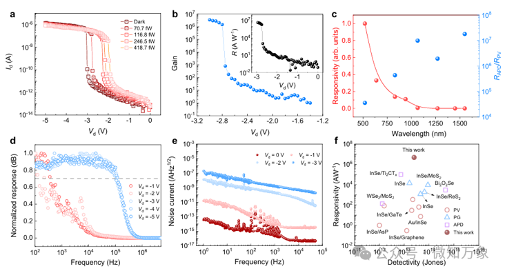 Figure 4.Photodetection characteristics at room temperature..Comment: It must be said that the structure and materials are not particularly novel; this kind of asymmetric structure is used in many devices. This work is also the first time it has been applied to avalanche diodes, but the key is that they have combined these not-so-new elements to create a device with very exaggerated performance metrics. This is unimaginable in traditional avalanche diodes that require tens of volts of high voltage. Moreover, being able to detect dozens of photons (about 35) at room temperature indicates that the device has excellent noise control. Therefore, although its approach (using asymmetric structures) and materials (two-dimensional materials) may not be original in other fields, the “product” it has achieved in this specific application indeed pushes the core metrics of gain and power consumption to a new height, showcasing the tremendous potential of this design strategy. It is unknown whether applying this structure to traditional materials with similar bandgaps would yield even better performance.
CHRISTMAS
Paper Link:
Zhao, D., Chen, Y., Hu, T. et al. Bilateral Geiger mode avalanche in InSe Schottky photodiodes. Nat Commun 16, 7859 (2025). https://doi.org/10.1038/s41467-025-62383-9
Note:
🔹 This article is for academic exchange among researchers only and is not for commercial use..
🔹 If there are any copyright issues with this article, please contact us in a timely manner..
🔹 Readers are welcome to share and promote this article to jointly promote the dissemination of research results..
🔹 “Micro Knowledge of All Things” will continue to strive to improve content quality, bringing readers higher-level interpretations of material research results. We look forward to your attention and support. We invite researchers to submit articles to share your latest research results and explore cutting-edge science with the global academic community!