Click the blue text to follow us
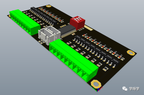
1. Basic Knowledge of Microcontroller I/O Expansion
1. Function of I/O Interface CircuitThe speed of external devices is very complex and must be implemented through the I/O interface circuit.(1) Speed CoordinationDue to the speed differences of various devices, the microcontroller cannot perform I/O operations synchronously at a fixed timing, but can only do so asynchronously, meaning that I/O operations can only proceed when it is confirmed that the device is ready for data transfer. Therefore, the interface circuit needs to generate status signals or interrupt request signals to indicate whether the device is ready. This is how the microcontroller coordinates speed with external devices via the interface circuit.(2) Output Data LatchingDue to the inconsistency in speed between the CPU and external devices, the interface circuit needs to latch the output data first and then transmit it once the output device is ready to receive the data. This is the data latching function of the interface circuit.(3) Data Bus IsolationMultiple data sources (input devices) and multiple data loads (output devices) may be connected on the line. When data transmission occurs between a pair of source and load, all other non-participating devices must be electrically isolated from the bus. This is the bus isolation function of the interface circuit.To achieve bus isolation, the interface circuit must provide a tri-state buffer circuit with tri-state buffering capability.(4) Data ConversionThere are various types of external devices, and the performance differences between different devices are significant, with diverse signal forms. The microcontroller can only use digital signals; if the external device provides or requires signals not in the form of voltage digital signals, an interface circuit is needed for conversion, including analog-to-digital conversion and digital-to-analog conversion.(5) Enhanced Driving CapabilityThe interface circuit provides sufficient driving power for the output data to ensure that external devices can operate normally and steadily.2. More Information About Interface Circuits(1) Interface and Interface CircuitAn “interface” has meanings such as a boundary and mutual connection, allowing two connected devices to work together. The microcontroller interface studies the connection issues between the microcontroller and external devices. The hardware circuit of the interface between the microcontroller and external devices is called the interface circuit, or I/O interface circuit.(2) Port or TerminalTo realize the interface function of the I/O interface circuit, the interface circuit should include some registers, which are usually referred to as ports or simply ports (Port) for those registers that are addressable and can perform read or (and) write operations. The complete interface function is achieved through a combination of hardware and software, while the port is the hardware content available for user use. When users perform extended connections and write related programs, they need to utilize various ports in the interface circuit, so they must know the settings and addressing of these ports.(3) Characteristics of I/O InterfacesThe complexity of external devices and I/O operations makes the interface circuit an essential interface between the microcontroller and external devices, coordinating and controlling to ensure the normal operation of external devices. The characteristics of I/O interfaces can be summarized as follows:① Asynchronous. The microcontroller and external devices usually work in parallel according to their respective timing, and only when needed does the external device accept control from the microcontroller through the interface circuit.② Real-time. The microcontroller controls external devices through polling or interrupt methods to maximize real-time control.③ Device Independence. The interface chip is not necessarily dedicated; the same interface chip can be configured for multiple devices through software.(4) Parallel and Serial InterfacesAccording to the different modes of data transmission, interfaces can be divided into parallel and serial interfaces, namely parallel interfaces and serial interfaces. This chapter focuses on parallel interfaces.3. I/O Addressing TechnologyTo perform read/write operations on the registers (ports) in the I/O interface circuit, addressing them is necessary, leading to the issue of I/O addressing. There are two I/O addressing methods: unified addressing and independent addressing. In the 80C51 microcontroller system, unified addressing is used.The so-called unified addressing method treats the registers in the I/O interface as equivalent to the storage units in the external extended data memory, using the same 64 KB external extended address space. The unified addressing of I/O and memory allows I/O ports to also use 16-bit address addressing and utilize data memory read/write instructions for I/O operations, eliminating the need for dedicated I/O instructions.The so-called independent addressing method separates I/O and memory addressing. Thus, in a microcontroller system, two independent address spaces are formed: memory address space and I/O address space. The advantage of the independent addressing method is that the two address spaces are clearly defined and independent, but it also presents many complications and increases system overhead, so the independent addressing method is less commonly used in microcontrollers.4. Microcontroller I/O Control Methods(1) Unconditional MethodUnconditional transmission, also known as synchronous program transmission, can only be used by devices that can always be prepared for I/O operations. When performing unconditional I/O operations, there is no need to test the device’s state; I/O operations can be performed at any time as needed.The unconditional transmission method is suitable for two types of devices. One type has permanent or slowly changing data signals, such as mechanical switches, indicator lights, LEDs, and digital tubes. The other type consists of devices that operate at very high speeds, sufficient to synchronize with the microcontroller, such as digital-to-analog converters (DACs).(2) Polling MethodThe polling method, also known as conditional transmission, requires checking the device’s state before I/O operations. The microcontroller can only execute I/O operations after confirming that the device is “ready.” This checking is also called “polling,” so this conditional I/O control method is referred to as the polling method.To implement polling-based I/O control, the interface circuit must provide the device state, and the status register or status bits in the interface circuit are prepared for this purpose. The polling method is only suitable for relatively small microcontroller systems.(3) Interrupt MethodThe main difference between the interrupt method and the polling method is how to determine whether the external device is ready for I/O operations. When using the interrupt method for I/O control, the device sends an interrupt request to the microcontroller once it is ready. Upon receiving the interrupt request, the microcontroller responds by pausing the currently executing program and switching to the interrupt service program, completing an I/O operation through the interrupt service program, and then returning to continue executing the original program that was interrupted.The interrupt method is more efficient, so it is widely used in microcontroller systems. However, since an interrupt request is an unpredictable random event, implementing it requires higher hardware and software requirements for the microcontroller system.2. Programmable Parallel Interface Chip 8255The 8255 is a product of Intel, known as a programmable interface chip because its operating mode and functions can be set and changed through programming.1. Hardware Logic Structure of 8255The full name of 8255 is “Programmable Parallel Input/Output Interface Chip,” which has strong universality and flexibility, suitable for expanding the parallel I/O ports of the 80C51 series microcontroller.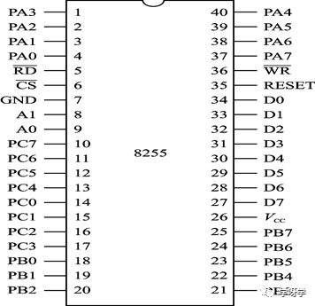
Pin Diagram of 8255 Chip
Based on functionality, the internal structure of 8255 can be divided into three logical circuit parts: port circuit, bus interface circuit, and control logic circuit, as shown in the figure below.
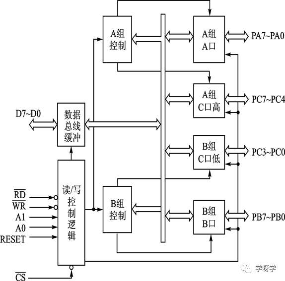
(1) Port Circuit8255 has a total of three 8-bit ports, where Port A and Port B are purely data ports. Port C can be used as both a data port and a control port, mainly used to implement the control functions of Port A and Port B. In practice, Port C is often divided into two parts: the high part (PC7 to PC4) and the low part (PC3 to PC0). The high part of Port C combined with Port A is referred to as Group A; the low part of Port C combined with Port B is referred to as Group B.(2) Bus Interface CircuitThe bus interface circuit is used to establish signal connections between the 8255 and the microcontroller chip. This includes:
- Data Bus Buffer. Data, control words, and status information related to I/O operations are transmitted through this buffer.
- Read/Write Control Logic. Relevant control signals include:
- /CS chip select signal (active low).
- /RD read signal (active low).
- /WR write signal (active low).
- A0, A1 low address signals for port selection. 8255 has four addressable ports.
- RESET reset signal (active high). After the chip is reset, the control register is cleared to 0, and all ports are set to input mode.
(3) Control Circuit for Group A and Group BThe control circuit for Group A and Group B together forms the control circuit of the 8255, which includes an 8-bit control register for storing programming commands and implementing control of each port operation.(4) Interrupt Control CircuitThe logic circuit of the 8255 also includes an interrupt control circuit. Each of the two ports A and B has an interrupt trigger in the interrupt control circuit, namely Trigger A and Trigger B, used to control the enable and disable of interrupts. Setting to enable and resetting to disable. The control of setting and resetting the two triggers is done through the relevant bits of Port C.2. Working Modes of 8255(1) Mode 0 (Basic Input/Output Mode)Mode 0 is suitable for unconditional data transfer. Both 8-bit ports (Port A and Port B) and two 4-bit ports (the high part and low part of Port C) can be set to Mode 0 separately or simultaneously.(2) Mode 1 (Strobed Input/Output Mode)Mode 1 is the strobed input/output mode. The “strobe” of 8255 is achieved through a “request” and “acknowledge” signal, realized in a handshake manner (also known as handshaking mode). Therefore, this data transmission method is conditional and is suitable for control performed via polling or interrupt. In Mode 1, Port A and Port B are data ports, while Port C is a control port used to transmit and save the handshake signals required by the data ports, which have specific definitions.(3) Mode 2 (Bidirectional Data Transfer Mode)Mode 2 adds bidirectional transfer functionality based on Mode 1, and only Port A can select this working mode. In this mode, Port A can both input and output data. If Port A is set to Mode 2, Port B can only operate in Mode 0. Mode 2 is suitable for bidirectional data transfer in polling or interrupt modes, requiring the use of the 5 lines of Port C as control lines.
Definition of Port C Handshake Signals
3. Programming Content of 8255The 8255 is a programmable interface chip, and its main programming content consists of two control commands, namely the working mode command and the Port C set/reset command.(1) Working Mode CommandThe working mode command is used to set the working mode and data transfer direction of each data port. The highest bit (D7) of the command is a flag bit, which is fixed at 1. The command format is shown in the figure below.Two points to note about the working mode command:
-
Port A has 3 working modes, while Port B only has two working modes;
-
In Modes 1 and 2, the definition of Port C (input or output) does not affect the functionality of the bits of Port C used as handshake signals.
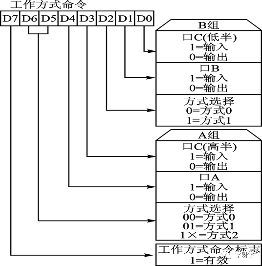 (2) Port C Set/Reset CommandIn Modes 1 and 2, Port C is used to define control signals and status signals, so each bit of Port C can be set or reset. The setting or resetting of the bits of Port C is performed by the set/reset command. The format of the 8255 set/reset command is shown in the figure below.
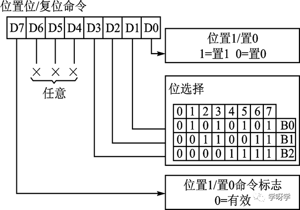 (3) Initialization ProgrammingThe initialization content of the 8255 involves writing commands to the control word register. For example, if the following settings are made for the 8255 ports: Port A Mode 0 input, Port B Mode 1 output, Port C high part output and low part input. Assuming the control register address is 0003H, according to the settings, the working mode command word would be 10010101, or 95H. The initialization program segment would be: MOV R0, #03H MOV A, #95H MOVX @R0, A
4. 8255 Interface Applications
(1) 8255’s I/O Control Methods
-
Unconditional Method
Using Mode 0 for data input/output is the unconditional transmission method.
-
Polling Method
In Modes 1 and 2, the polling method can be used for data transmission. The status signal for polling during data input is IBF (for Port A it is IBFA, for Port B it is IBFB), as the lines transmitting these signals are PC5 and PC1, so polling involves testing the state of the input lines.
During data output, the status signal for polling is OBF (for Port A it is OBFA, for Port B it is OBF), and the tested lines are PC7 and PC1.
-
Interrupt Method
In Modes 1 and 2, the interrupt method can also be used for data transmission. The interrupt request signal is INTR (for Port A it is INTRA, for Port B it is INTRB), and the lines transmitting the interrupt request signals are PC3 and PC0.
(2) Port Selection and Read/Write Control
8255 has a total of four addressable ports: Port A, Port B, Port C, and control register, selected by the combination of CS and the states of address lines A0 and A1, and controlled by the read/write signals RD and WR. The specific settings are shown in the table below.
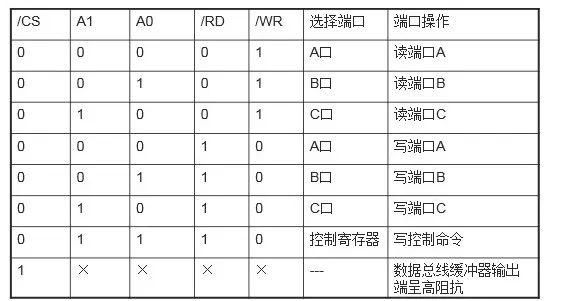
8255 Port Selection and Read/Write Control Table
3. Keyboard Interface Technology
The keyboard is an essential human-computer interaction device for microcontrollers.
1. Key Scanning and Key Code Generation
(1) Keyboard Example
To illustrate the working principle of the keyboard, take an 8-row × 4-column matrix keyboard as an example, as shown in the figure below.
The keyboard has row lines and column lines, with a total of 8 row lines and 4 column lines. At the intersection of the row and column lines, there is a key. Since the row lines and column lines are connected to different ends of the key, the key remains open under normal conditions, so the row and column lines do not connect. During interfacing, one end of the row line connects to the output port, while the other end is left floating; the column line connects one end through a resistor to a +5 V power supply and the other end to the input port. Since the column line is connected to the +5 V power supply through a resistor, its initial state is high level.
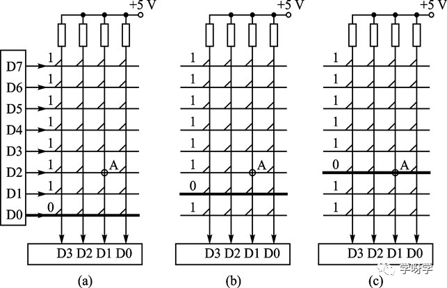
Keyboard Scanning Diagram
(2) Key Code
Each key on the keyboard is responsible for a processing function, and this function is implemented through software. Therefore, the keyboard interface must have software support. Each key corresponds to a processing program segment, and the function of the key is realized by running this program segment. To smoothly branch to the key processing program segment in the program, each key needs to be encoded, referred to as a key code, so that program branching can occur based on the key code. There is no unified standard for key encoding, and various key encoding methods exist. The most common encoding method is to encode the keys based on their positions in the keyboard matrix, starting from 0 in natural number order, with key codes represented in hexadecimal. The table below shows the key codes for the keys in the keyboard scanning diagram, where the first column on the left corresponds to the scanning codes for each row, and the last row shows the status codes (or return codes) when a key in the corresponding column is closed. The content in the table represents key codes, noting the regularity of the arrangement of key codes.
(3) Keyboard Scanning
Typically, the keys pressed on the keyboard are referred to as closed keys. To identify closed keys, there are two methods available: row scanning and line inversion, with the row scanning method being commonly used in microcontrollers, referred to as the scanning method. The keyboard scanning introduced here is implemented through software. The keyboard scanning process is driven by a scanning program, so the scanning process is also the execution process of the scanning program. Before starting, the program repeatedly checks for closed keys, i.e., whether there are any closed keys on the keyboard. To do this, all row lines should output 0, and then the column line state is read back. If the column line state is all 1, it indicates that no key is pressed; if not all 1, it indicates that a key is pressed. When a key is pressed, the row and column lines connect at the intersection of the closed key, causing the corresponding column line to become low level. Upon detecting a closed key, the scanning process continues to determine which key is closed; if no closed key is detected, the program returns to repeat the search for closed keys. The scanning process involves sequentially outputting a low level from each row line and then inputting the column line state to determine whether any closed keys exist. Upon detecting a closed key, the scanning does not end immediately; it continues to check if other keys are pressed simultaneously until all row lines output 7FH.
(4) Debouncing
Whenever a key press is confirmed, debouncing should be performed. This is because when a key is pressed, due to the elasticity of the mechanical contacts and voltage fluctuations, there will be voltage bouncing during the moment the contacts close and release. Debouncing can be handled through software and hardware methods. The software debouncing method uses a time delay to avoid bouncing (with a delay time of 10 to 20 ms being sufficient), while the hardware method involves adding a debouncing circuit to the keyboard to suppress bouncing, which may include using bistable circuits or filtering circuits, but hardware debouncing increases costs.
2. Implementing Keyboard Interface with 8255
(1) Interface Circuit Logic Diagram
Taking the 8255 as the interface for an 8×4 keyboard as an example. Port A is the output port connected to the keyboard row lines. Port C is the input port, with PC3 to PC0 connected to the keyboard’s 4 column lines. Assuming the address of Port A is 8000H, then the address of Port B is 8001H, the address of Port C is 8002H, and the control register address is 8003H.
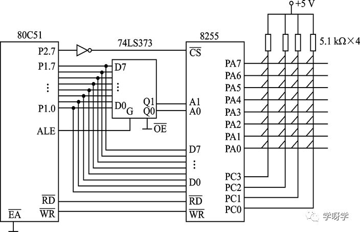
(2) Subroutine to Check for Closed Keys
The subroutine to check for closed keys is KS, which can be called in the keyboard scanning program. The result of executing the KS subroutine is: if there is a closed key, then (A) ≠ 0; if there is no closed key, then (A) = 0. The program is as follows:
KS: MOV DPTR, #8000H
MOV A, #00H ; Port A sends 00H
MOVX@DPTR, A
INC DPTR
INC DPTR ; Establish C port address
MOVXA, @DPTR ; Read C port
CPL A ; A is inverted, if no key is pressed, then all are 0
ANL A, #0FH ; Mask the high half byte of A
RET
(3) Keyboard Scanning Program
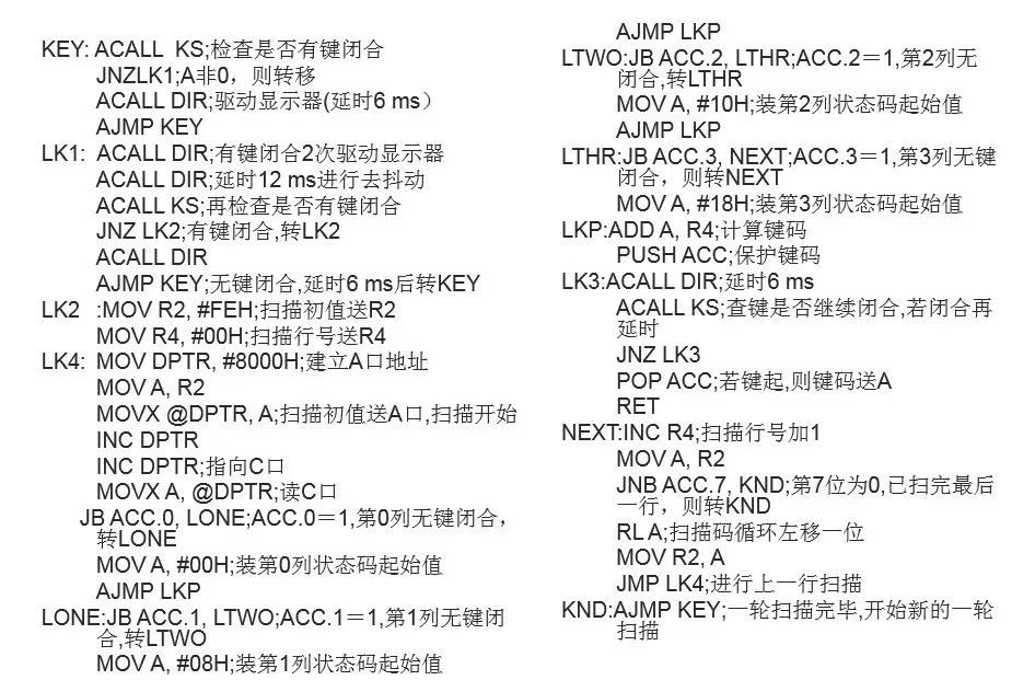
In microcontroller application systems, keyboards and displays often coexist, so the keyboard program and display program can be combined, using the display program as a delay subroutine within the keyboard program. This way, it does not delay the display drive while also allowing timed scanning of the keyboard.
Assuming the display driver program is DIR, with an execution time of about 6 ms. The keyboard scanning program is as follows, where R2 is the scanning code register and R4 is the row counter.
4. LED Display Interface Technology
In microcontroller application systems, the simplest and most common display device is the LED display.
1. Overview of LED Displays
LED stands for Light Emitting Diode, which is an electroluminescent device that converts electrical signals into light signals.
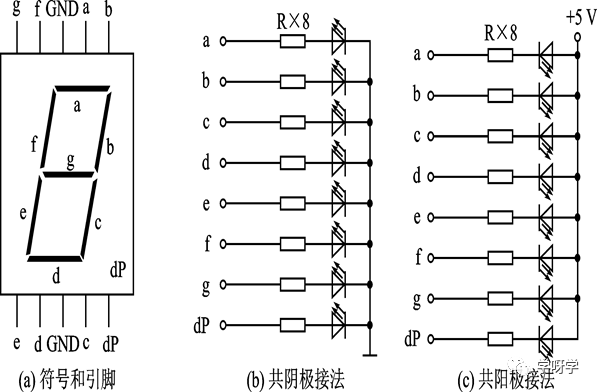
There are 7-segment and 8-segment LED displays. A 7-segment display consists of 7 light-emitting diodes, while an 8-segment display adds a round light-emitting diode (indicated as dp in the figure) to display the decimal point. The arrangement of the light-emitting diodes in an 8-segment display is shown in the figure below (a).
8-segment LED displays are widely used due to many characteristics, including:
① Fast light response, strong brightness, and good high-frequency characteristics; moreover, depending on the materials used, the displays can emit various colors such as red, yellow, green, blue, and orange.
② Good mechanical properties, small size, light weight, low cost; compatible with CMOS and TTL circuits; long service life, reaching 105 to 106 hours.
③ Low operating voltage and moderate driving current. The working current for each segment is 5 to 10 mA, and to fully illuminate a 7-segment display requires a current of 35 to 70 mA. Such a large current needs to be provided by a driving circuit, so care should be taken regarding the driving issues of the display.
When used, to apply driving voltage to the light-emitting diodes, they should have a common pin, which can be connected in the following two ways:
① Common Cathode Connection. The cathodes of the light-emitting diodes are connected together to form a common cathode pin, as shown in the figure (b). When used, the common cathode pin is grounded, so light-emitting diodes with a high level on the anode pin will turn on, while those with a low level will not.
② Common Anode Connection. The anodes of the light-emitting diodes are connected together to form a common anode pin, as shown in the figure (c). When used, the common anode pin is connected to +5 V, so light-emitting diodes with a low level on the cathode pin will turn on, while those with a high level will not.
2. Display Principle of LED Displays
(1) Segment Code
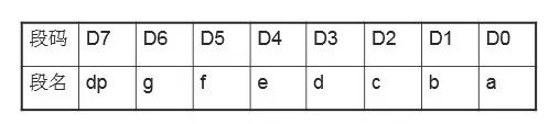
The segment code refers to the state combinations of each segment provided for displaying on the digital tube, namely the character code. The segment code for a 7-segment display consists of 7 bits, while for an 8-segment display, it consists of 8 bits, which can be represented by a single byte. In the segment code byte, the code bits correspond to the relationship with each segment’s light-emitting diodes as shown below:
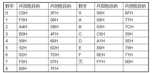
The values of the segment codes depend on the connection method of the display’s common pin (common anode and common cathode). Taking the 8-segment display as an example, the segment code values for displaying hexadecimal numbers are shown in the table below.
(2) Dynamic Display Method of LED Displays
Multiple digit displays used in parallel are referred to as LED displays. LED displays commonly use dynamic display methods, where all digit displays share a single set of segment code driving circuits. During display, the digit displays are sequentially illuminated through a scanning method, cycling through each display. Although only one digit display is illuminated at any given moment, due to the human eye’s persistence of vision effect, it appears as if all digit displays are continuously illuminated. Dynamic display of LED displays requires providing segment codes and corresponding position control, which is commonly referred to as segment control and position control.
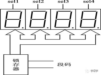
3. LED Display Interface
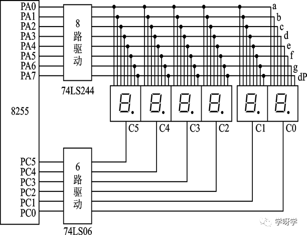
(1) Implementing LED Display Interface with 8255
The following diagram shows the interface circuit using the 8255 for a 6-digit LED display. Port PC is the position code output port, with PC5 to PC0 outputting position control lines. Due to the large driving current, the output is connected to a 74LS06 to invert and increase driving capability. Port PA is the segment code output port, with the load current of each segment code line being approximately 8 mA. To enhance display brightness, a 74LS244 is connected for segment control output driving.
When using the 8255 for the LED display interface, 8255 can only output display segment codes without control functions; dynamic control must be implemented through programming. There are two points to note regarding this:
① To store segment codes, it is common to set up a display buffer in the internal RAM of the 80C51, with the number of storage units equal to the number of LED display digits, where each unit corresponds to one display position.
② To ensure display brightness during the scanning process, each digit display should remain illuminated for a period of time (approximately 1 ms) to stabilize its brightness. Therefore, a time delay should be added between each digit during the scanning process.
(2) LED Display Driver Program
Assuming Port A address is 8000H, Port B address is 8001H, then Port C address is 8002H, and control register address is 8003H. The LED display position control port address is 8002H, and segment control port address is 8000H. The LED display program is as follows, where R0 stores the current position control value and DL is the delay subroutine.
DIR: MOV R0, #79H; Establish display buffer starting address
MOVR3, #01H; Start display from the right
MOVA, R3; Initial value of position control code
LD0:MOV DPTR, #8002H; Position control port address
MOVX@DPTR, A; Output position control code
MOVDPTR,#8000H; Segment control port address
MOVA, @R0; Fetch display data
DIR0:ADD A, #0DH
MOVC A, @A+PC; Lookup character code
DIR1:MOVX @DPTR, A; Output segment control code
ACALLDL; Delay
INCR0; Move to the next buffer unit
MOVA, R3
JBACC.5, LD1; Check if reached the highest position; if so, return
RLA; If not, shift to the high position
MOVR3, A; Save position control code in R3
AJMPLD0; Continue scanning
LD1:RET
DSEG: DBC0H; Character code table
DBF9H
DBA4H
5. Printer Interface Technology
1. Overview of Micro Printers
Micro printers used in microcontroller systems often adopt low-cost and easy-to-interface designs.
The μP series printers can be connected to microcontrollers via a flat 20-pin cable, with the signals as follows:
DB7 to DB0 — Data lines, with data transmission being unidirectional, i.e., from the microcontroller to the printer.
STB — Data select signal, a low-level valid input signal for the printer. When this signal is active, print data is sent to the printer, and at its rising edge, the data is latched.
BUSY — Printer “busy” signal, a status signal output by the printer. ACK — Printer acknowledgment signal, active low. This signal indicates that the printer has finished processing the received data, notifying the microcontroller that new data can be sent.
ERR — Error signal output by the printer.
2. Printer Interface
(1) Direct Connection Between Microcontroller and Printer
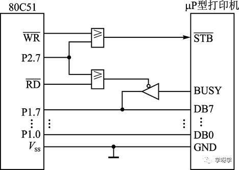
Since the printer interface signals are relatively few, the printer interface is simple, and it can even be directly connected to the microcontroller without an interface circuit, as shown in the figure below.
The 8 data lines of the printer are directly connected to Port 1 of the 80C51, using one address line (P2.7) to enable the read signal /RD and write signal /WR of the 80C51. The enabled /WR signal connects to the printer’s STB signal, and the enabled /RD signal controls the printer’s BUSY (sending to Port 1.7).
In the printer, there is only one data register for storing print data. Only address line P2.7 is used, with the data port address being 7FFFH.
For the connection method shown in the figure, it is only suitable to use the polling method for printer control, i.e., polling the state of the BUSY signal. If the interrupt method is to be used, the ACK signal should be used as the interrupt request, connecting the ACK signal to the external interrupt pins INT0 or INT1 of the 80C51.
(2) Using 8255 as Printer Interface
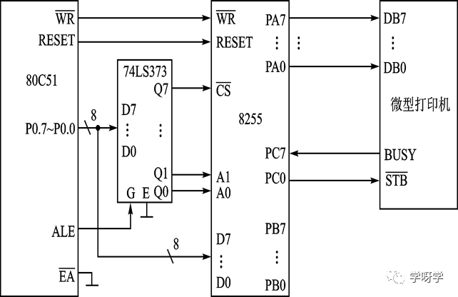
If the resources of the 80C51 are tight, an interface chip is needed to connect to the printer, for example, using the 8255 as the printer interface chip, as shown in the figure below.
The connection between the 8255 and the 80C51 adopts line selection method for I/O addressing, using P0.7 as the chip select signal for the 8255. The two lowest address bits are connected to the port selection terminals A0 and A1 of the 8255. Assuming that the unconnected addresses are all set to 1, the address of Port A of the 8255 is 7CH, Port B address is 7DH, Port C address is 7EH, and control register address is 7FH.
For the connection between the 8255 and the printer, if the polling method is used for print control, the connections between the 8255 and the printer are:
-
Port A (PA7 to PA0) is connected to the printer data lines for transmitting print data.
-
C port’s PC0 provides the data select signal, connected to the printer’s STB terminal, for controlling the selection of print data to the printer.
-
C port’s PC7 is connected to the printer’s BUSY terminal, using BUSY as the state polling signal.
The working mode command word for the 8255 can be determined as 10001000 (88H).
Port A is set to Mode 0 output, D6D5D4 = 000;
Port B is unused, assuming D2D1 = 00;
Port C high bit is input, D3 = 1;
Port C low bit is output, D0 = 0.
8255 as Printer Interface
(3) Print Driver Program
To write the print driver program, a buffer is set up in the internal RAM for storing print data. Two parameters are set: one is the starting address of the buffer R1, and the other is the length of the buffer R2. The data select signal STB sent to the printer is a negative pulse, which is generated at the PC0 terminal after the print data is sent from the microcontroller to the 8255.
MOVR0, #7FH ; Control register address
MOVA, #88H; Working mode command
MOVX@R0, A ; Write working mode command
TP: MOVR0, #7EH ; C port address
TP1:MOVX A, @R0 ; Read C port
JBACC.7, TP1; BUSY=1, continue polling
MOVR0, #7CH ; A port address
MOVA, @R1; Fetch data from buffer
MOVX@R0, A ; Send print data to 8255
INCR1 ; Point to the next unit
MOVR0, #7FH ; Control port address
MOVA, #00H; Output STB pulse
MOVX@R0, A
MOVA, #01H
MOVX@R0, A
DJNZR2, TP ; Decrease data length by 1, if not 0 continue
RET

Long press the picture to follow
Discover more exciting content
WeChat ID: Mechanical-knowledge