ver0.2
Introduction
In previous articles, we introduced the core content of the power management system architecture and software architecture under the ARM architecture, and conducted a thorough analysis of the idle management mechanism of the PE-Core, PSCI. Another important branch of OSPM for PE-Core power management is DVFS, which maximizes the efficiency of the PE-Core through OSPM intervention. This article will discuss the topic of DVFS, clarifying the system architecture related to DVFS, laying the hardware foundation for our subsequent discussions on OSPM scheduling (performance) management, etc. Before reading this article, we hope everyone will read our previous articles to grasp some basics and get a feel for the content:
(1)[V-02] Basics of Virtualization – CPU Architecture (Based on AArch64)
(2)[A-03] ARMv8/ARMv9 – Multi-level Cache Architecture
(3)[A-21] ARMv8/v9 – Overview of SMMU System Architecture and Functions
(4)[A-25] ARMv8/v9 – System Architecture of GIC (Hardware Foundation of Interrupts)
(5)[A-38] ARMv8/v9 – Generic Timer System Architecture
(6)[A-41] ARMv9/v8 – Power Management System Architecture
(7)[A-42] ARMv9/v8 – Overview of Power Management Working Principles (SCP Service Overview)
(8)[A-43] ARMv9/v8 – Introduction to Power Control Framework (PCF)
(9)[A-0x2c] ARMv9/v8 – Power Management Domains (Voltage Domain/Power Domain)
(10)[A-45] ARMv9/v8 – Power Modes
(11)[A-46] ARMv9/v8 – Power States
(12)[V-05] Basics of Virtualization – Exception Model (AArch64)
(13)[A-47] ARMv9/v8 – Software Architecture for Power State Management (PSCI Architecture)
(14)[A-48] ARMv9/v8 – Power State Management Mechanism (PSCI Coordination Mechanism)
(15)[A-49] ARMv9/v8 – Overview of PSCI Interface Specification and Workflow
Body
1.1 Background
Remember how we introduced how OSPM intervenes in power management under the PSCI framework:
OSPM for AP cores can be broadly classified into idle management and dynamic voltage and frequency scaling (DVFS) frameworks. As shown in Figure 1-0, these frameworks are associated with the scheduling in the OS. However, it should be noted that the association between the scheduler and the OSPM frameworks might only be a loose coupling.
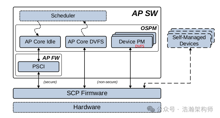
Figure 1-0 Simplified power management software stack
This article will discuss the DVFS-related content under the PSCA framework from the perspective of system architecture. The main focus will be on the system architecture level, with some discussions on the software level interspersed. The core DVFS software modules will be shared in subsequent articles in conjunction with specific OS (Linux).
1.2 Components Related to DVFS
1.2.1 Core Hub of SCP-DVFS
First, let’s look at the core node SCP under the PSCA architecture, as shown in Figure 1-1.
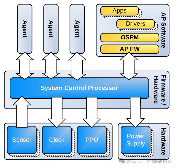
Figure 1-1 System Control Processor concept
The main four control points of SCP for power management of SOC based on ARM architecture are Sensor, Clock, Processor, and Power Supply, while the managed objects are various Agents on the SOC, including the CPU as an Agent. SCP has many functions, including the following two aspects:
Voltage Regulator Control
The SCP manages voltage supplies for functions including post-boot switch-on, switch off, and DVFS voltage level changes.
The voltage supplies are typically provided by a separate power management IC. The voltage regulator control component provides the interface for this function. The protocol of the interface is implementation-specific, dependent on the choice of power management IC.
Clock Control
The SCP does not control runtime dynamic gating of clocks at the component activity level. This is managed by clock controllers with hardware autonomous Q-Channel management.
The SCP manages clock source enabling, selection, and division. Clock sources might include off-chip sources, such as crystal oscillators, and on-chip sources such as PLLs. Each clock source will typically be able to be divided to produce a multitude of frequencies for different components.
These settings might be static, set up once when a component is required or powered up, or changed at the request of the component or related software, such as for AP or GPU DVFS.
From the above description, we can summarize two points:
(1) The voltage control content of SCP for various Agents within the system includes: startup, shutdown, and voltage level adjustment (DVFS voltage level changes). ARM’s PSCA integration manual also provides an introduction to the components for adjusting voltage, as shown in Figure 1-2:
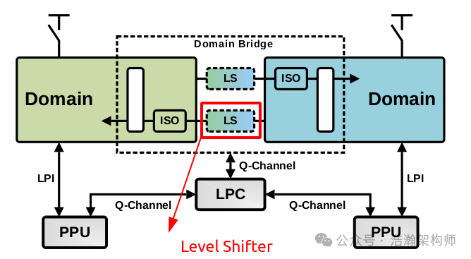
Figure 1-2 Voltage Level Shifter
Let’s look at the manual’s description of LS:
When crossing between voltage domains, level shifters must be placed between the two domains to manage the difference in voltage levels between the two voltage supplies. Closing timing across such a boundary is difficult because of the considerable number of voltage-supply cross corners that need to be analyzed. Therefore, it is treated as an asynchronous interface for all signals.
(2) The management of Clock by SCP mainly includes enabling, selecting, and dividing clock sources. The framework for clock management under the PSCA system is shown in Figure 1-3:
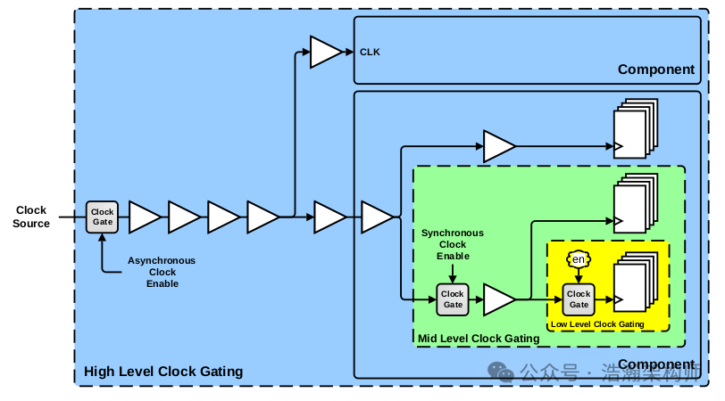
Figure 1-3 Clock gating hierarchy
Looking at the manual’s description, the core point is that through a hierarchical clock management architecture, it is possible to flexibly and efficiently control the power performance of various power domains within the SOC through clock control. This part will not be discussed further:
There can be multiple levels of clock gating within a system. This specification uses the following classification:
• Low-Level: Clock gates inserted automatically by synthesis tools.
• Mid-Level: Instantiated clock gating, typically synchronously controlled, within components.
• High-Level: Instantiated gating of entire clock domains.
These clock gating levels are all complementary and should be implemented regardless of the presence of other levels within the structure. Each level has benefits with different levels of power saving and temporal granularity.
From the above description, it can be seen that the PSCA framework supports dynamic adjustment of voltage levels and clock frequencies, which lays the hardware foundation for our continued discussion on DVFS.
1.2.2 PE-Cores – The Objects of DVFS Operations
For ARM’s CPU, OSPM achieves optimal energy efficiency for PE-Cores through DVFS adjustments:
Many systems operate under conditions where their workload is variable. Therefore, it is useful to be able to reduce or increase the core performance to match the expected core workload.
Clocking the core more slowly reduces dynamic power consumption.
Dynamic Voltage and Frequency Scaling (DVFS) is an energy-saving technique that exploits:
• The linear relationship between power consumption and operational frequency.
• The quadratic relationship between power consumption and operational voltage. This relationship is given as:
P = C × V × V × f
Where:
P Is the dynamic power.
C Is the switching capacitance of the logic circuit in question.
V Is the operational voltage.
f Is the operational frequency.
Power savings are achieved by adjusting the frequency of a core clock.
At lower frequencies, the core can also operate at lower voltages. The advantage of reducing supply voltage is that it reduces both dynamic and static power.
There is an IMPLEMENTATION SPECIFIC relationship between the operational voltage for a given circuit and the range of frequencies that circuit can safely operate at. A given frequency of operation together with its corresponding operational voltage is expressed as a tuple and is known as an Operating Performance Point (OPP). For a given system, the range of attainable OPPs is collectively termed as the system DVFS curve.
Operating systems use DVFS to save energy and, where necessary, keep within thermal limits. The OS provides DVFS policies to manage the power consumed and the required performance. A policy that is aimed at high performance selects higher frequencies and uses more energy. A policy that is aimed at saving energy selects lower frequencies and therefore results in lower performance.
From the formula above, it can be seen that a working voltage and a working frequency directly determine the power consumption of the ARM CPU. Here we summarize the adjustments of voltage and clock as follows:
(1) First, the ARM CPU must implement the basic components of the PSCA framework, allowing each PE-Core to support DVFS adjustments by SCP at runtime. Here we take the DSU as an example for explanation.
• Voltage Adjustment
The voltage adjustment is carried out on a voltage domain basis, as shown in Figure 1-4:
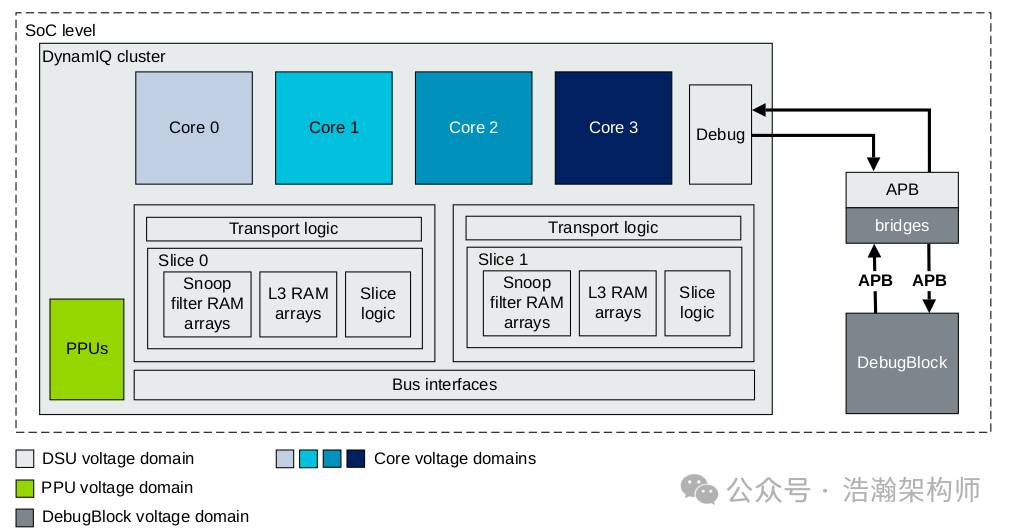
Figure 1-4 DSU-120 voltage domains
Excerpt from the DSU manual:
The power management techniques employed by the DSU-120 and cores in the cluster include:
• Power Policy Units (PPUs) providing autonomous power management of the L3 cache and the cores
• Support for cores running independently at different frequencies and voltages known as Dynamic Voltage Frequency Scaling (DVFS). For cores in a complex, DVFS is only possible for the whole complex, not for individual cores.
• Per-core Dynamic Voltage and Frequency Scaling (DVFS)
• Having each core in a separate voltage domain allows Dynamic Voltage Frequency Scaling (DVFS) to be applied to each core.
This part is actually quite understandable. The DSU cluster and the PE-Cores under this cluster support DVFS adjustments based on different combinations, either individually or as a group, and the basis for voltage adjustment is to place these PE-Cores in different voltage domains.
• Clock Adjustment
With the basis for voltage adjustment established, it’s time for clock adjustment, as shown in Figure 1-5:
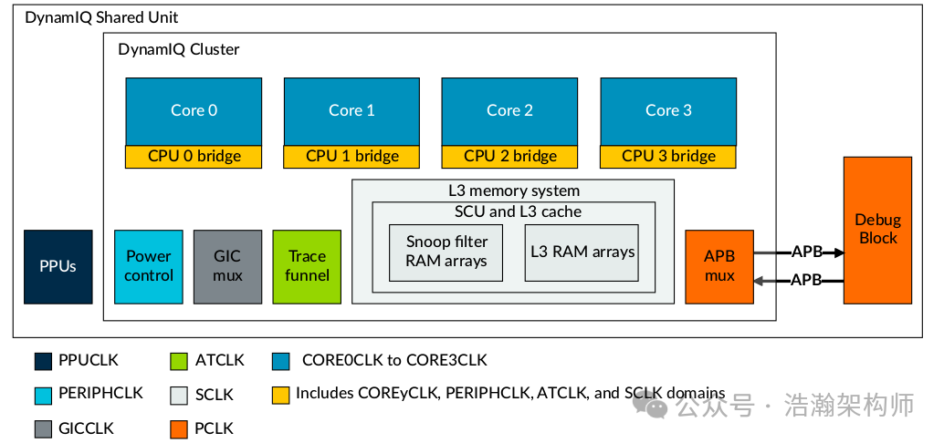
Figure 1-5 DSU-120 clock domains
Let’s look at the manual’s description:
The DynamIQ ™ Shared Unit-120 (DSU-120) has multiple clock domains. Each core or complex can be implemented in a separate clock domain.
The cluster contains several clock domains for functionality that is likely to be connected to different clocks in the system. Within each core, the CPU bridge contains asynchronous bridges for all crossings between the core and cluster clock domains.
ARM categorizes each component within the DSU into a clock domain, and different clock signals naturally have different effects, as shown in Figure 1-6:
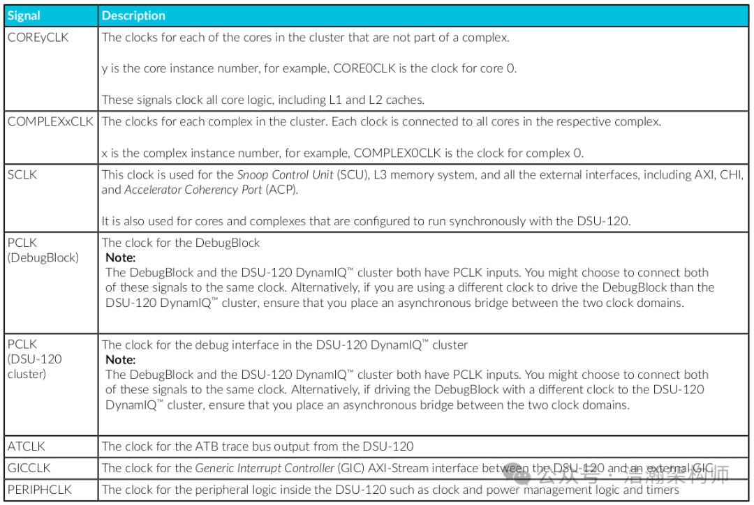
Figure 1-6 DSU-120 clock signals
Combining Figures 1-5 and 1-6, we focus on the clocks related to the PE-Core:
While there is no functional requirement for any of the clocks to have any relationship to any of the others, the DSU-120 is designed with the following expectations to achieve acceptable performance:
• The COREyCLK or COMPLEXxCLK can be dynamically scaled to match the performance requirements of that core.
• SCLK is recommended to run between the maximum COREyCLK or COMPLEXxCLK frequency and approximately half of the maximum COREyCLK or COMPLEXxCLK frequency.
• SCLK can run at synchronous 1:1 or 2:1 frequencies with the external interconnect, avoiding the need for an asynchronous bridge between them.
• The frequency of ATCLK must be determined based on the trace bandwidth of the system.
• GICCLK can be run at the same frequency as the interrupt controller that it connects to. This would typically be approximately 25% of the maximum COREyCLK or COMPLEXxCLK frequency.
• PCLK can run at the same frequency as the debug subsystem that it connects to. This would typically be approximately 25% of the maximum COREyCLK or COMPLEXxCLK frequency.
• The PERIPHCLK domain contains the architectural timers, and software performance can be impacted if reads to these registers take too long. Therefore, Arm ® recommends that the PERIPHCLK frequency is at least 25% of the maximum COREyCLK or COMPLEXxCLK frequency.
• Arm ® recommends that the PPUCLK clock frequency is at least 25% of the maximum COREyCLK or COMPLEXxCLK frequency. When implementing the retention power state controls for retention power and operating modes, retention entry and exit latency is limited by the PPUCLK clock frequency.
This part will not be discussed further; the core point is that the clocks related to the PE-Core need to support clock frequency adjustments, naturally to meet performance requirements in different scenarios.
(2) Now that the infrastructure for adjusting the voltage and clock frequency of the PE-Core is in place, how do we adjust it?
Workload performance is typically equated to CPU clock frequency, and a corresponding voltage to drive the clock at the selected frequency. A CPU core or cluster of CPU cores can operate at one or more **{frequency, voltage}** pairs. Each such pair is called an Operating Performance Point (OPP), and the related performance management scheme is referred to as Dynamic Voltage and Frequency Scaling (DVFS) or Dynamic Clock and Voltage Scaling (DCVS). This framework allows workload performance to be set and measured in terms of distinct and discrete OPPs. This requires the OS kernel to possess full knowledge of the OPP values that the platform supports and recognize how they are read and set. Each SoC offers different methods for reading and setting OPPs. Furthermore, some SoCs offer additional means of controlling performance, which have similar power and performance tradeoffs, such as CPU throttling.
An alternative to the OPP-based DVFS approach is to view performance as a continuum of performance levels in an abstract, linear scale. The SCP can map individual OPPs to equivalent performance levels in this scale and then expose the performance scale and levels to the OS. The DVFS framework in the OS can then be built on top of this abstract scale, making the OS code platform-agnostic. This facilitates kernel code development, generalization, distribution, maintenance, and porting.
Through the OPP mechanism, voltage and clock frequency pairs are stored within the OSPM system, and then different OPPs are selected based on different application scenarios to notify SCP to set them to the PE-Core. Here we excerpt a code snippet from the Linux DTS (if the chip vendor has standardized the integration of ARM chips well, it can even achieve decoupling of OPP at the EL1 level in the system), helping everyone to get a feel for it, as shown in Figure 1-7:
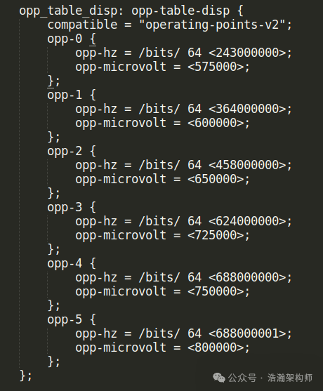
Figure 1-7 Linux OPP Table
In fact, the PSCA integration manual for SOC has already made corresponding considerations, as shown in Figure 1-8:
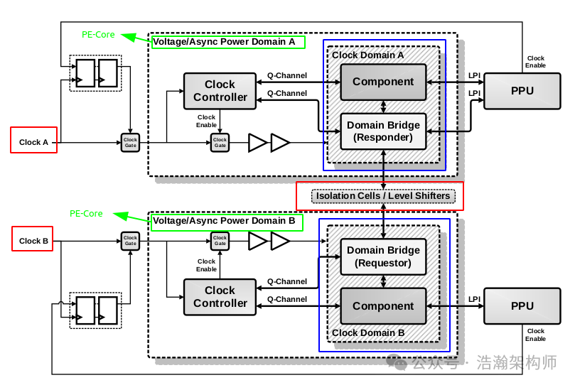
Figure 1-8 Voltage or asynchronous-power domain boundary example
The operation of SCP on the OPPs passed from OSPM is actually an operation on the Clock Domain and Voltage Domain. If the PE-Core falls within these two Domains at this time, then an OPP setting operation can be completed. We simplify Figure 1-8 as shown in Figure 1-9, which may make it easier for everyone to understand.
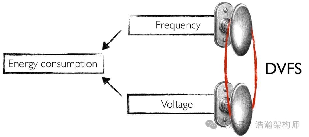
Figure 1-9 DVFS Demo
Adjusting the main frequency must be accompanied by voltage adjustment. A higher main frequency means the CPU has to do more work, which requires more energy, thus necessitating a higher voltage. Higher voltage means higher power consumption, which leads to more heat generation. For electronic components, heat can change their electrical characteristics, and exceeding limits may cause irreversible damage. Therefore, the configuration and selection of OPP is a task that requires repeated calibration.
(3) So can OSPM use the DVFS mechanism without limits? The answer is no. Regardless of any OPP issued by OSPM, SCP will make a decision based on the system state it knows before determining the next action. The most important factor to consider here is Thermal, aimed at protecting hardware resources from damage due to OSPM’s strong performance demands. This monitoring task is usually completed by SMCF, as shown in Figure 1-10:
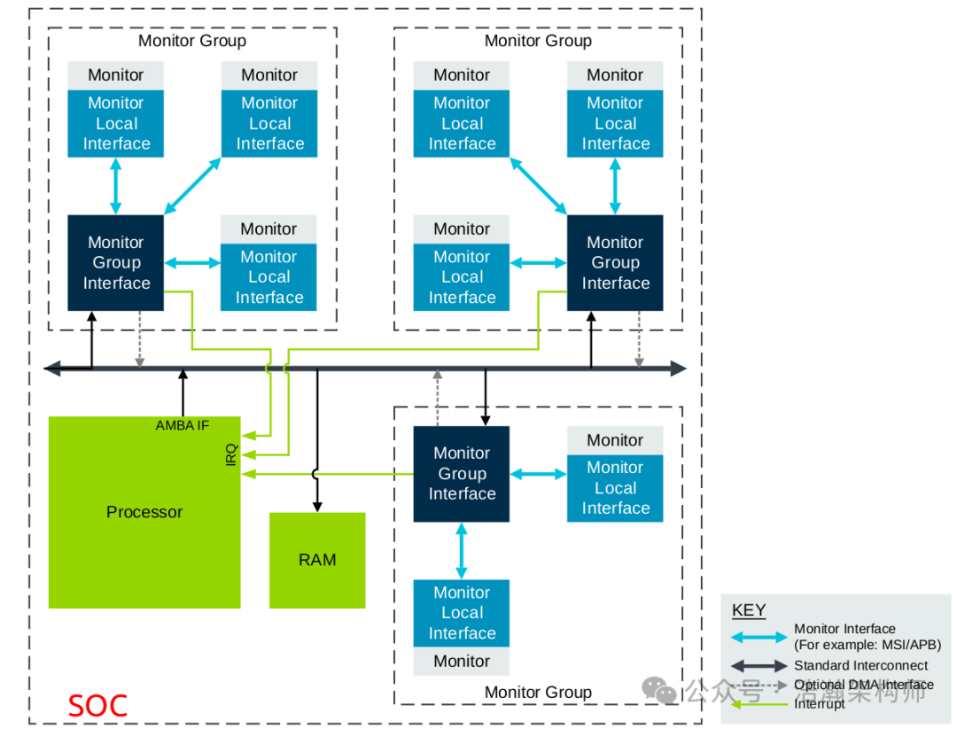
Figure 1-10 System Monitor Control Framework overview
We will not discuss SMCF here; interested friends can refer to the relevant manual. Here we excerpt part of the manual’s content:
The System Monitoring Control Framework is designed to manage a large and diverse set of on-chip sensors and monitors. It does this by presenting software with a standard interface to control the monitors, regardless of type, and reducing the software load of controlling the monitor sampling and data collection.
The SMCF reduces the burden on monitor control by enabling sampling on multiple monitors to be controlled together and by various triggers either internal or external to the SMCF. The number of monitors that the SMCF supports can be configured.
The SMCF eases data collection requirements by allowing the data from multiple monitors to be collated in a single location or writing out data to a memory-mapped location that is easier for the monitoring agent to access.
The SMCF can also reduce the requirement on the monitoring agent to constantly monitor data by providing programmable alerts that can inform the monitoring agent when certain changes happen or thresholds are crossed.
The monitoring agent is only required to perform an initial setup and then process data when required on a constant basis or when an alert informs it that analysis or action is required.
The structure of the SMCF is one of distributed monitor groups located around the system where monitoring is required, reusing existing interconnect infrastructure where applicable to communicate.
1.3 DVFS and GPU
Above, we introduced the objects of DVFS operations mainly focused on PE-Cores, but other IPs on the bus can also support DVFS:
A primary motivation for additional voltage domains is to support DVFS for functional areas of the SoC. DVFS is a fundamental technique for both energy and performance optimization. While initially used for AP cores, it is increasingly being applied to other components of the SoC.
Graphics processing performance in mobile applications has grown significantly and is anticipated to continue. GPU workloads represent throughput processing, with very high inherent parallelism, and are well suited to using DVFS to adapt the performance and energy profile of a given hardware configuration to a frame level deadline.
These properties also enable adaptation to different requirements. Cost-centric designs can implement fewer cores at higher frequency and voltage, while energy-performance-centric designs can implement more cores at lower frequency and voltage.
Therefore, a dedicated voltage domain to enable GPU DVFS is often implemented to enable these benefits.
In applications where DVFS is not required, or the cost is considered to outweigh the benefit, then the GPU cluster is in the V SYS domain.
Here we provide a specific example to help everyone understand the manual regarding the support of DVFS by graphic chips, such as MALI-GPU:
GPU utilization counters provide an alternative view of the data path activity cycles, normalizing the queue usage against the total GPU active cycle count. These metrics provide a clearer view of breakdown by workload type and the effectiveness of queue scheduling.
Mobile systems improve energy efficiency by using Dynamic Voltage and Frequency Scaling (DVFS) to reduce voltage and clock frequency for light workloads. When seeing a workload with high percentage utilization, check the GPU active cycles counter to confirm the frequency. A highly utilized GPU might look like a problem, but it can be caused by a light workload running at a low clock frequency.
A shader core consists of multiple parallel processing units. Performance counters can track utilization and workload characteristics for all the major processing units, allowing developers to find both bottlenecks and content inefficiencies to optimize.
For shader-bound content, the functional unit with the highest loading is likely to be the bottleneck. To improve performance, you can reduce the number of operations of that type in the shader. Alternatively, reduce the precision of the operations to use 8 and 16-bit types so that multiple operations are performed in parallel.
For thermally bound content, reducing the critical path load gives the biggest gain as it allows use of a lower operating frequency. However, reducing load on any functional unit helps improve energy efficiency.
This part will not be discussed further; the core point is that the GPU’s workload scenarios have become increasingly demanding with the iteration of SOC, and considering user experience, energy efficiency control has also become very important. Therefore, introducing DVFS technology is a necessary means to enhance energy efficiency. However, the microarchitecture of GPU and CPU cores still has significant differences. Here we attach a diagram of the MALI GPU-Core for comparative research, as shown in Figure 1-11:
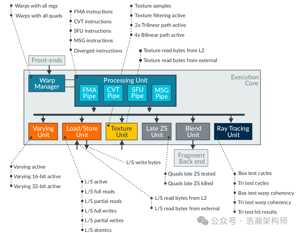
Figure 1-11 Valhall GPU shader core
1.4 DVFS System Architecture
With the previous groundwork laid, let’s summarize the DVFS system architecture, as shown in Figure 1-12:
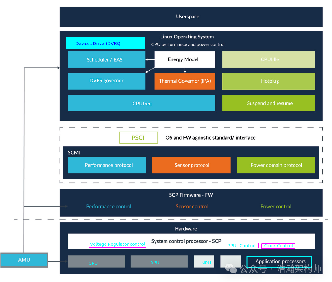
Figure 1-12 DVFS System ARCH
Combining the above figure, we summarize the DVFS system architecture as follows:
(1) From the software perspective, DVFS management policies can work on any Agent under the PSCA framework, but in most cases, only Agents that require fine-grained power control will apply DVFS strategies. Most of the applications of DVFS strategies are on the CPU node. Other IPs on the bus, such as GPUs, can also use DVFS strategies for energy consumption control based on configuration, but usually, these strategies do not make decisions internally within DVFS but are managed by device drivers running on the CPU. Clearly, the CPU has more information and can more easily make correct decisions based on user intent. For example, if a user launches a 3D application on the CPU, the GPU needs to quickly increase its main frequency.
(2) On the software level, DVFS cannot work in isolation; usually, OSPM will have a complete Energy Model to predict and manage the energy efficiency within the entire OS. This EM is the brain that controls the entire SOC power subsystem. On one hand, it needs to collect data from system Sensors, and on the other hand, it needs to consider the load of various TASKs within the system. Finally, it sends the power strategy after decision-making through the CPU’s Power agent module or device drivers to the hardware, such as OPP.
(3) The PSCA framework has already provided sufficient infrastructure to help OSPM complete DVFS operations, such as Regulators, Clocks, PPUs, etc. The core control node is still SCP. As the link between OSPM and hardware, we need to consider how to accurately convey OSPM’s intentions to various IPs on the bus, and also consider how to reduce maintenance costs to facilitate continuous iteration of SOC. ARM provides a good solution by standardizing the ARM SOC development process, and for DVFS, it addresses these issues through the SCMI mechanism, which we will continue to discuss later.
Conclusion
In this article, we started with the functions of SCP regarding voltage and clock control, gradually expanding to the infrastructure supporting DVFS operations for PE-Cores (power domains and clock domains), and then extended the core principles of DVFS operations through the introduction of the OPP mechanism. Subsequently, we introduced the support of other bus IPs for the DVFS mechanism, such as graphic chips, which now need to support DVFS to achieve energy efficiency. Finally, we extracted the system architecture during DVFS operations from the PSCA framework based on the Linux system. Power management and system performance have always been closely related, and DVFS is the cornerstone of performance optimization. We hope that through this article, we can help everyone open the door to research on performance optimization. That’s all for today, thank you all, please follow, share, and comment.
Reference
[01] <DEN0050D_Power_Control_System_Architecture.pdf>
[02] <armv8_a_power_management_100960_0100_en.pdf>
[03] <Power_Policy_Unit_Architecture_Specification_0051E.pdf>
[04] <DEN0024A_v8_architecture_PG.pdf>
[05] <79-LX-LD-s003-Linux设备驱动开发详解4_0内核-3rd.pdf>
[06] <80-PGxxx-35_QNX_Thermal_Manager_Overview.pdf>
[07] <80-pgxxx-7_n_qnx_power_management_software_architecture_reference_manual.pdf>
[08] <80-ARM-POWER-HK0001_一文搞懂ARM_SoC功耗控制架构.pdf>
[09] <Arm_Power_and_Performance_Management_SCMI_White_Paper.pdf>
[10] <80-ARM-POWER-cs0001_Arm-SoC-power功耗控制架构.pdf>
[11] <80-LX-LK-cl0009_深入理解Linux电源管理.pdf>
[12] <DEN0056D_System_Control_and_Management_Interface_v3_1.pdf>
[13] <arm_total_compute_2021_reference_design_software_developer_guide_en.pdf>
[14] <arm_total_compute_2022_reference_design_software_developer_guide_en.pdf>
[15] <arm_cortex_m85_processor_trm_en.pdf>
[16] <DEN0108_00eac0_smcf-archl-Specification.pdf>
[17] <DEN0022F.b_Power_State_Coordination_Interface.pdf>
[18] <MTxxxx_SCP_User_Manual_V1.0.pdf>
[19] <learn_the_architecture_arm_system_architectures_en.pdf>
[20] <arm_dsu_110_trm_101381_0400_11_en.pdf>
[21] <DEN0077A_Firmware_Framework_Arm_A_profile_1.1_EAC0.pdf>
[22] <80-LX-POWER-PSCI-cs0001_Linux-PSCI框架.pdf>
[23] <learn_the_architecture_realm_management_extension_guide.pdf>
[24] <ISA_A64_xml_A_profile-2024-03.pdf>
[25] <learn_the_architecture_aarch64_memory_management_guide.pdf>
[26] <IHI0069H_gic_architecture_specification.pdf>
[27] <DEN0044H_ArmBBR_2.1Final.pdf>
[28] <LVC20-118-0-SCMI-server-in-TEE.pdf>
[29] <trustedfirmware-a-readthedocs-io-en-latest.pdf>
[30] <arm_mali_g615_performance_counters_reference_guide.pdf>
Glossary
AP – application processor
OSPM – Operating System Power Management
WFI – Wait For Interrupt
WFE – Wait For Event
DVFS – Dynamic Voltage and Frequency Scaling
SCU – Snoop Control Unit
OPP – Operating Performance Point
PSCI – Power State Coordination Interface
PPU – Power Policy Unit
PCSA – Power Control System Architecture
SoC – System-on-Chip
PCF – Power Control Framework
SCP – System Control Processor
BSP – board support package
SCMI – System Control and Management Interface
EAS – Energy Aware Scheduling
IPA – Intelligent Power Allocation
ACPI – Advanced Configuration and Power Interface
LPI – Low-Power Idle
CPPC – Collaborative Processor Performance Control
PCSM – power control state machine
AOSS – Always-on subsystem
PMIC – Power Management Integrated Circuit
JM – job manager
AON – always on domain
SBSA – Server Base System Architecture
CLK_CTRL – Clock Controller
LPD – Low Power Distributor
LPC – Low Power Combiner
P2Q – P-Channel to Q-Channel Convertor
GPIO – General Purpose IO
RAS – Reliability, Availability, and Serviceability
STR – Suspend to RAM
SMCCC – SMC Calling Convention
RMM – Realm Management Monitor
BMC – board management controller
PPF – Privileged platform firmware
SPM – Secure Partition Manager
SP – Secure Partition
DCVS – Dynamic Clock and Voltage Scaling
V-BSA – Virtual Base System Architecture
BBR – Base Boot Requirements