ver0.3
Introduction
Those who have persisted in reading this article are already remarkable, as they now understand the weak memory ordering architecture of ARM. You not only understand the types of memory, the memory sharing mechanisms, and the memory consistency mechanisms, but also the CPU architecture and the microarchitecture of processors, all of which lay a solid foundation for explaining today’s topic. The upgrade of processors is directed towards three aspects: faster, higher, and stronger. “Faster” means a higher clock frequency, allowing more instructions to be executed in a single clock cycle; “Higher” means that the processor PE-Core introduces more hardware mechanisms to ensure that the “faster” performance can be fully utilized, such as the ARM weakly ordered memory model mentioned earlier; “Stronger” refers to richer processing capabilities at the functional level, such as floating-point calculations and vector calculations. From the perspective of the PE-Core, more hardware capabilities mean more efficient code execution, and these optimization mechanisms act like an invisible hand controlling the execution of program instruction flows. However, these mechanisms can introduce a certain degree of uncertainty into the computing world. This uncertainty is directly manifested as memory reordering, which is not always desirable. For example, in the field of automotive functional safety, the interaction between systems and components must be seamless without any inconsistencies. At this point, the ARM architecture needs to provide corresponding mechanisms for developers to design programs that ensure reliability. This mechanism acts like a tangible hand controlling the execution of the entire system. Now, let us delve into the main topic of this article: the memory barrier mechanism.
Main Content
1.1 Observer
Before introducing the memory barrier mechanism, we need to understand an important concept: the Observer. Although we have introduced a lot of background knowledge related to this article in previous articles, it is still necessary to spend some time clarifying the definition of an Observer, as this greatly aids our understanding of the ARM memory barrier mechanism.
1.1.1 Concept of Observer
First, let’s look at the ARM manual’s description of an Observer:
Observer: A PE or mechanism in the system, such as a peripheral device, that can generate reads from or writes to memory.
• An Observer refers to either a Processor Element (PE) or some other mechanism in the system, such as a peripheral device, that can generate reads from, or writes to, memory. Observers can observe memory accesses.
• The ARM Architecture Reference Manual defines certain key words, in particular, the terms observe and must be observed. In typical systems, this defines how the bus interface of a master, for example, a core or GPU and the interconnect, must handle bus transactions. Only masters are able to observe transfers. All bus transactions are initiated by a master. The architecture considers the following as separate Observers:
• The instruction interface of the core, typically called the Instruction Fetch Unit (IFU)
• The data interface, typically called the Load Store Unit (LSU)
• The MMU table walk unit
As described in Who is an Observer?, an Observer is something that can make memory accesses. For example, the MMU generates reads to walk translation tables.
While writing this article, I consulted many materials to find a precise definition of what an Observer is within the ARM architecture. It was quite frustrating, but then I realized that I should just present what I found, as there are certainly smart people among the readers who can provide insights, haha.
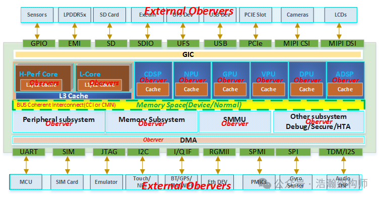 Figure 1-1 High-Level ARM SOC ARCH
Based on the manual’s description and Figure 1-1, we can summarize the characteristics that an Observer in the ARM architecture must possess.
(1) An Observer must be a functional unit within the SOC system, such as a PE, GPU, VPU, DMA controller, etc.
(2) An Observer can also be further subdivided into more refined functional units within the PE, such as MMU or LSU.
(3) An Observer must be associated with the system’s memory model, observing memory spaces of both Device and Normal types.
(4) An Observer can be understood as an alias for the Master concept in the SOC bus architecture, focusing more on memory operation-related bus transactions.
(5) Observers are interconnected, and consistency handling is necessary when required (which can be done either in hardware or software).
We can simply understand that functional units with the above characteristics in an SOC can be considered as Observers within the ARM architecture. Here, we can extend this to devices outside the SOC, as they can also be considered Observers in the ARM architecture from a certain perspective, since they are indirectly connected to the SOC bus through peripheral interfaces, and their behavior can also indirectly generate bus transactions.
1.1.2 Observability
In the previous section, we introduced Observers within the ARM architecture, which are essentially a group of Masters revolving around memory. This raises the question: what exactly are these Observers doing during the operation of the system? What are they observing? When do they observe? Let’s first look at the manual’s description.
The order that a master performs transactions in is not necessarily the same order that such transactions complete at the slave device, because transactions might be re-ordered by the interconnect unless some ordering is explicitly enforced.
A write to memory is observed when it reaches a point in the memory system in which it becomes visible. When it is visible, it is coherent to all the Observers in the specified Shareability domain, as specified in the memory barrier instruction. If a PE writes to a memory location, the write is observable if another PE would see the updated value if it read the same location. For example, if the memory is Normal cacheable, the write is observable when it reaches the coherent data caches of that Shareability domain.
A simple way to describe observability is to say that “I have observed your write when I can read what you wrote and I have observed your read when I can no longer change the value you read,” where both I and you refer to cores or other masters in the system.
We can directly conclude:
(1) These Observers must first be grouped, observing the shared memory within their respective memory sharing domains.
(2) The specific content of observation has two aspects:
• One is behavior, which refers to whether the shared memory is written to or read by the Observer.
• The other is the result, which is from the perspective of an Observer operating on shared memory, regarding when other Observers in the shared domain can see this result.
(3) The factual result can be expressed in another way: observability.
• A PE is an Observer. When a PE-Core-A writes data to a memory address, it takes several instruction cycles to complete, and only when another PE-Core-B can see this result does it represent that the write action of PE-Core-A is observable and perceivable. Conversely, when PE-Core-B reads data from this address, PE-Core-A can capture it and cannot change the current data value, which represents that PE-Core-B’s read action can be perceived.
The core idea of the above section is that reading and writing shared memory data must go through a process; whether writing or reading, it must be in an observable state for the shared data, otherwise, the consequences are on the user.
1.1.3 Order
In the previous section, we discussed that reading and writing shared data between Observers must be synchronized, meaning they must be in an observable state to obtain valid data that expresses the intentions of other Observers. Clearly, this requires a mechanism to ensure a certain order of memory operations between Observers; otherwise, under the ARM weakly ordered memory model, there will still be lingering concerns. Let’s look at the manual’s description:
While the effect of ordering is largely hidden from the programmer within a single PE, the microarchitectural innovations have a profound impact on the ordering of memory accesses. Write buffering, speculation, and cache coherency protocols, in particular, can all mean that the order in which memory accesses occur, as seen by an external observer, differs significantly from the order of accesses that would appear in the SEM. This is usually invisible in a uniprocessor environment, but the effect becomes much more significant when multiple PEs are trying to communicate with memory. In reality, these effects are often only significant at particular synchronization boundaries between the different threads of execution.
The memory discussed in the manual has been repeatedly covered in previous articles, and here we summarize again: the world of memory requires barriers.
1.2 Memory Barriers (Barrier)
A memory barrier, also known as a memory fence or synchronization barrier, is an instruction used to enforce the order of memory accesses and synchronize events. In modern computer systems, especially in multiprocessor or multicore systems, memory barriers are a crucial concept. The ARM architecture, as one of the mainstream architectures for mobile devices and embedded systems, also provides memory barrier mechanisms to ensure data consistency and the correct execution order of instructions.
The Arm architecture is a weakly ordered memory architecture that supports out-of-order completion. Memory barrier is the general term applied to an instruction, or sequence of instructions, that forces synchronization events by a PE with respect to retiring load/store instructions. The memory barriers defined by the architecture provide a range of functionality, including:
• Ordering of load/store instructions.
• Completion of load/store instructions.
• Context synchronization.
The following subsections describe the Arm memory barrier instructions:
• Instruction Synchronization Barrier (ISB).
• Data Memory Barrier (DMB).
• Speculation Barrier (SB).
• Consumption of Speculative Data Barrier (CSDB).
• Speculative Store Bypass Barrier (SSBB).
• Profiling Synchronization Barrier (PSB).
• Physical Speculative Store Bypass Barrier (PSSBB).
• Trace Synchronization Barrier (TSB).
• Data Synchronization Barrier (DSB).
• Shareability and access limitations on the data barrier operations.
• Load-Acquire, Load-AcquirePC, and Store-Release.
• LoadLOAcquire, StoreLORelease.
• Guarded Control Stack Barrier (GCSB).
In the ARM architecture, the memory barrier mechanism primarily prevents the processor from executing memory accesses out of order, ensuring data consistency and the correct order of instructions. We do not intend to introduce all these instructions one by one; instead, we will focus on three widely recognized instructions (DMB, DSB, ISB) to help everyone understand the basic principles of how memory barriers work in the ARM architecture.
1.2.1 Data Memory Barrier (DMB)
First, let’s look at the manual’s description:
The Data Memory Barrier (DMB) prevents the reordering of specified explicit data accesses across the barrier instruction. All explicit data load or store instructions, which are executed by the PE in program order before the DMB, are observed by all Observers within a specified Shareability domain before the data accesses after the DMB in program order.
Only after all memory access operations before it have been completed can the access instructions after it be committed. The DMB instruction guarantees the order of all memory access instructions before and after the DMB instruction. In other words, memory access instructions after the DMB instruction will not be reordered by the processor to occur before the DMB instruction. The DMB instruction does not guarantee that memory access instructions before the memory barrier instruction must complete; it only guarantees the execution order of memory access instructions before and after the memory barrier instruction. The DMB instruction only affects memory access instructions, data cache instructions, and cache management instructions, and does not affect the order of other instructions.
Let’s explain DMB with an example:
(1) As shown in Figure 1-2, an Observer (PE-Core-A) executes the following instruction stream, assuming the initial values of addresses X1 and X3 are 0x0.
 Figure 1-2 Without using memory barrier mechanism
(2) If we do not implement any barrier measures for Observer (PE-Core-A), then when Observer (PE-Core-B) initiates a read access to the shared data, it may generate the following contexts, as shown in Figure 1-3.
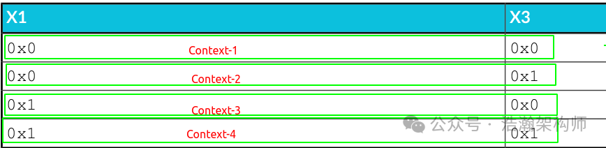 Figure 1-3 Context without using memory barrier mechanism
Context-1:
• Observer (PE-Core-A) has not executed any operations on the shared data.• Or Observer (PE-Core-A) has performed operations, but they are not completed, and other Observers cannot observe Observer (PE-Core-A)’s write operations (X1 & X3 are not in an observable state).• Observer (PE-Core-B) has performed a read operation on the shared memory.
Context-2:
• Observer (PE-Core-A) has reordered, and X3 has been modified.
• Observer (PE-Core-A) has not performed operations on X1, or the operations on X1 are not completed, and other Observers cannot observe Observer (PE-Core-A)’s write operations (X1 is not in an observable state).
• Observer (PE-Core-B) has performed a read operation on the shared memory.
Context-3:
• Observer (PE-Core-A) has completed the write operation on X1.
• Observer (PE-Core-A) has not started or completed the write operation on X3 (X3 is not in an observable state).
• Observer (PE-Core-B) has performed a read operation on the shared memory.
Context-4:
• Observer (PE-Core-A) has completed the write operations on X1 and X3.
• Observer (PE-Core-B) has performed a read operation on the shared memory.
(3) For the code snippet in Figure 1-2, if we add the memory barrier DMB, while keeping other conditions unchanged.
 Figure 1-4 Using memory barrier mechanism
(4) If we implement barrier measures for Observer (PE-Core-A), then when Observer (PE-Core-B) initiates a read access to the shared data, it may generate the following contexts, as shown in Figure 1-5.
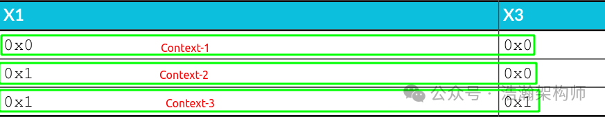 Figure 1-5 Context using memory barrier mechanism
Context-1:
• Observer (PE-Core-A) has not executed any operations on the shared data.
• Or Observer (PE-Core-A) has performed operations, but they are not completed, and other Observers cannot observe Observer (PE-Core-A)’s write operations (X1 & X3 are not in an observable state).
• Observer (PE-Core-B) has performed a read operation on the shared memory.
Context-2:
• Observer (PE-Core-A) has completed the operation on X1, and has not started or completed the operation on X3 (X3 is not in an observable state).
• Observer (PE-Core-B) has performed a read operation on the shared memory.
Context-3:
• Observer (PE-Core-A) has completed the operations on X1 and X3.
• Observer (PE-Core-B) has performed a read operation on the shared memory.
Through the above small experiment, we can see that after using DMB, Observer (PE-Core-A) will not perform reordering optimizations on the operation of X3, thus ensuring that other Observers, such as Observer (PE-Core-B), observe the order of operations on X1 and X3 by Observer (PE-Core-A). However, at this point, it only guarantees the order and does not guarantee the effective result of Observer (PE-Core-A)’s operation on X1.
1.2.2 Data Synchronization Barrier (DSB)
First, let’s look at the manual:
A DSB is a memory barrier that ensures that those memory accesses that occur before the DSB have completed before the completion of the DSB instruction. In doing this, it acts as a stronger barrier than a DMB. All the ordering that a DMB creates with specific arguments is also generated by a DSB with the same arguments.
A DSB that is executed by a PE completes when:
• All explicit memory accesses of the required access types that appear in program order before the DSB are complete for the set of observers in the required Shareability domain.
• If the argument specified in the DSB is reads and writes, then all cache maintenance instructions and all TLB maintenance instructions that are issued by the PE before the DSB are complete for the required Shareability domain.
DSB is stricter than the DMB instruction; only after all access instructions before it have been completed can the instructions after it be executed, meaning any instruction must wait for the access instructions before the DSB to complete. All caches, such as branch prediction and TLB maintenance operations, before this instruction must be completed. This can be illustrated with an example, as shown in Figure 1-6:
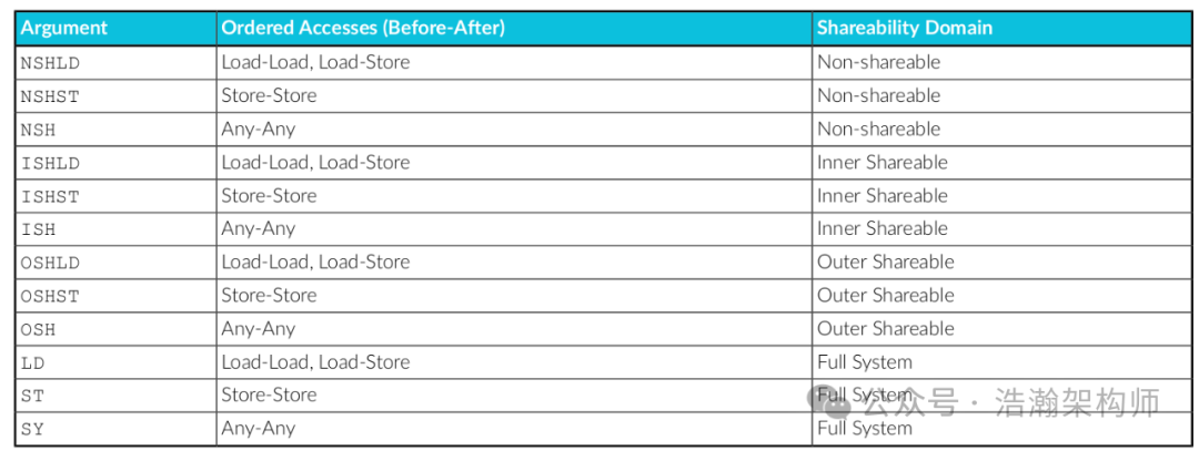 Figure 1-6 Using memory barrier DSB
In the above example, if DMB is used, then the ADD instruction can still be reordered within the current Observer (PE-Core), but after using DSB, ADD will never execute before the DSB, and its execution condition is still to wait for the current Observer (PE-Core) to complete the operation on X1.
Completion
The difference between DSB and DMB is relatively easy to understand, but to fully grasp it, one must understand what execution completion means.
Let’s look at a simple version:
The completion of a read is easier to explain than the completion of a write. This is because the completion of a read is the point at which read data is returned to the architectural general-purpose registers of the PE.The completion of a write is more complicated. For a write to Device memory, the point at which the write is complete depends on the Early-write acknowledgment attribute that is specified in the Device memory type, as described in Device memory in the Armv8-A memory model guide. If the memory system supports Early-write acknowledgment, then the DSB can retire before the write has reached the end peripheral. A write to memory that is defined as Device-nGnRnE can only complete when the write response comes from the end peripheral.
To summarize simply:
(1) The concept of memory access completion is divided into “read completion” and “write completion”.
(2) The criterion for “read completion” is that the relevant data has passed through the storage subsystem of the PE-Core to reach the execution units (EUs) of the back-end.
(3) “Write completion” is more complex and needs to be judged based on specific situations, but it also requires relevant feedback signals to be sent to the back-end EUs to be considered complete.
The above is a simple version; in reality, the scenarios within the ARM architecture are more complex, and the criteria for judgment vary based on context. Here, we only quote some of the original rules from the manual without further discussion.
For all memory, the completion rules are defined as:
• A Memory Read effect R1 to a Location is complete for a shareability domain when all of the following are true:
— Any write to the same Location by an observer within the shareability domain will be Coherence-after R1.
— Any translation table walks associated with R1 are complete for that shareability domain.
• A Memory Write effect W1 to a Location is complete for a shareability domain when all of the following are true:
— Any write to the same Location by an observer within the shareability domain will be Coherence-after W1.
— Any read to the same Location by an observer within the shareability domain will either Reads-from W1 or Reads-from a Memory Write effect that is Coherence-after W1.
— Any translation table walks associated with the write are complete for that shareability domain.
• A translation table walk is complete for a shareability domain when the memory accesses, including the updates to translation table entries, associated with the translation table walk are complete for that shareability domain, and the TLB is updated.
• A cache maintenance instruction is complete for a shareability domain when the memory effects of the instruction are complete for that shareability domain, and any translation table walks that arise from the instruction are complete for that shareability domain.
• A TLB invalidate instruction is complete when all memory accesses using the TLB entries that have been invalidated are complete.
Scope
DSB and DMB also have their own working scopes, as shown in Figure 1-7:
Figure 1-7 Using memory barrier DSB
When parameters are assigned to the DSB and DMB instructions, the effective range of the memory barrier is established, as shown in Figure 1-8:
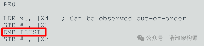 Figure 1-8 Specifying the scope of memory barriers
In the example, the barrier instruction is assigned the parameter ISHST, indicating that the effective area is only the Observers within Inner Shareable, and only storage operations are of concern. At this point, the following contexts can occur:
(1) Non-storage operation instructions in the code snippet can be reordered within the current Observer-PE0.
(2) The order of other Observers within the current Inner Shareable observing shared data X1 and X3 remains unchanged.
(2) Observers outside the current Inner Shareable can observe shared data X1 and X3 in any order, meaning X3 may take effect before X1.
1.2.3 Instruction Synchronization Barrier (ISB)
First, let’s look at the manual:
This is used to guarantee that any subsequent instructions are fetched, again, so that privilege and access are checked with the current MMU configuration. It is used to ensure any previously executed context-changing operations, such as writes to system control registers, have completed by the time the ISB completes. In hardware terms, this might mean that the instruction pipeline is flushed, for example. Typical uses of this would be in memory management, cache control, and context switching code, or where code is being moved about in memory.
The ISB instruction waits for all previous instructions to complete and flushes the cache in the instruction pipeline, refreshing the instruction prefetch queue to ensure that the executed instructions are the latest versions, thus ensuring that subsequent instructions are executed in the correct order. Using ISB can prevent the execution of erroneous or invalid instructions during execution. In scenarios involving changes to program state, flushing instruction caches, or ensuring the order of instructions, ISB is used to refresh the instructions in the pipeline, ensuring that subsequent instructions are executed in the correct order. It is stricter than DMB and DSB instructions and is typically used to guarantee the effects of context switching, such as VMID, ASID changes, TLB maintenance operations, etc. This part involves a vast topic of ARM context switching, which we will plan a dedicated article for; here we will not elaborate further.
1.3 Usage Scenarios of Memory Barriers
We will briefly outline two concrete scenarios to help everyone further understand the principles of how memory barriers work.
(1) Data synchronization in multithreaded programming
In multithreaded programming, multiple threads may simultaneously access shared data. To ensure the correctness and consistency of the data, memory barrier instructions need to be used to ensure the order of access to shared data. For example, after updating shared data, using DMB or DSB instructions ensures that the updates are visible to other threads, as shown in Figure 1-9.
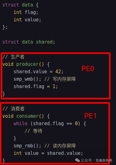
Figure 1-9 Memory barriers in multithreaded programming
In this example, we define PE0 and PE1 as a group of Observer groups. In PE0, smp_wmb() ensures that the write of value is completed before the write of flag, while in PE1, smp_rmb() ensures that the read of flag is completed before reading value. Without these memory barriers, the processor or compiler may reorder these operations, leading to consumers potentially reading uninitialized or partially initialized data.
(2) Register access in device drivers
In device driver programming, read and write operations to device registers need to be performed in a strict order. Using memory barrier instructions can ensure the order and synchronization of read and write operations to device registers, thus avoiding potential errors and side effects.
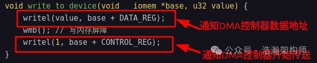 Figure 1-10 Memory barriers in drivers
In this example, we assume that the PE-Core executing the driver code and the DMA controller form a group of Observer groups. At this point, vmb() ensures that the starting address of the data block to be transferred by the DMA is observed by the DMA Controller before the instruction to start sending is executed, ensuring that the DMA controller will send the correct data block during the transfer.
Conclusion
In addition to the content introduced above, the ARM memory barrier mechanism has many points worth studying:
(1) Operations on certain system registers can also affect the order seen by Observers.
(2) More application scenarios for memory barriers, such as context switching, memory management, and synchronization in multiprocessor systems.
(3) Performance considerations for memory barriers and how to use them reasonably.
(4) What are the application scenarios for the standards of memory execution completion.
(5) And more.
Due to the author’s limited time and expertise, I cannot present everything to everyone. I hope this article can serve as a starting point to spark interest in ARM technology among more friends, encouraging them to join in the research. A friend left a message saying they were afraid to ask questions for fear of sounding unprofessional… I want to say that in a group of three, there must be a teacher for me; knowledge is gained through repeated learning, and abilities can only be improved through continuous communication. Truth can only be revealed through reflection and practice. Everyone should not be afraid of making mistakes; be bold like the author to gain something. Please stay tuned.
Reference
[00] <corelink_dmc520_technical_reference_manual_en.pdf>
[01] <corelink_dmc620_dynamic_memory_controller_trm.pdf>
[02] <IP-Controller/DDI0331G_dmc340_r4p0_trm.pdf>
[03] <80-ARM-IP-cs0001_ARMv8基础篇-400系列控制器IP.pdf>
[04] <arm_cortex_a725_core_trm_107652_0001_04_en.pdf>
[05] <DDI0487K_a_a-profile_architecture_reference_manual.pdf>
[06] <armv8_a_address_translation.pdf>
[07] <cortex_a55_trm_100442_0200_02_en.pdf>
[08] <learn_the_architecture_aarch64_memory_management_guide_en.pdf>
[09] <learn_the_architecture_armv8-a_memory_systems_en.pdf>
[10] <79-LX-LK-z0002_奔跑吧Linux内核-V-2-卷1_基础架构.pdf>
[11] <79-LX-LD-s003-Linux设备驱动开发详解4_0内核-3rd.pdf>
[12] <learn_the_architecture_memory_systems_ordering_and_barriers.pdf>
[13] <arm_dsu_120_trm_102547_0201_07_en.pdf>
[14] <80-ARM-MM-AL0001_内存学习(三):物理地址空间.pdf>
[15] <80-LX-MM-cs0002_Linux内存屏障.pdf>
Glossary
MMU – Memory Management Unit
TLB – translation lookaside buffer
VIPT – Virtual Index Physical Tag
VIVT – Virtual Index Virtual Tag
PIPT – Physical Index Physical Tag
VA – Virtual Address
PA – Physical Address
IPS – Intermediate Physical Space
IPA – Intermediate Physical Address
VMID – virtual machine identifier
TLB – translation lookaside buffer(地址变换高速缓存)
VTTBR_EL2 – Virtualization Translation Table Base Registers
ASID – Address Space Identifier (ASID)
DMC – Dynamic Memory Controller
DDR SDRAM – Double Data Rate Synchronous Dynamic Random Access Memory
TBI – Top Byte Ignore
DMB – Data Memory Barrier
DSB – Data Synchronization Barrier
ISB – Instruction Synchronization Barrier
DSU – DynamIQ ™ Shared Unit
SOC – System on Chip