Click the blue text to follow us
Follow and star our public account for exciting content delivered daily

Source: Online materials
The reconfigurability of FPGAs brings high flexibility, so designs/products based on FPGAs often have the need for updates/upgrades later on. However, due to physical constraints, FPGA boards that need updates/upgrades may not be able to be upgraded on-site. For example:
1. FPGA boards deployed in remote data centers cannot be accessed at any time for upgrades (the cost of traveling back and forth and restrictions on access to the data center).
2. FPGA boards deployed in relatively complex environments, such as wireless communication devices placed on communication towers, or devices in the hands of customers that cannot be collected and upgraded by suppliers one by one.
3. FPGA upgrades can significantly impact the system, making it inconvenient to upgrade at any time. For example, PCIe devices are monitored by the system bus, and arbitrary updates may cause the machine to restart, which is not allowed in some strictly regulated environments.
Therefore, there is a demand for remote updates of FPGAs, which must meet the following constraints:
1. Remote upgrades can be performed under certain conditions (such as available network for remote access), and while full automation is not necessary, it is more convenient if it is automated;
2. The update process must not impact the system to prevent the system from incorrectly implementing protective measures (e.g., server restarts);
Remote updates can be divided into two main parts: 1) data transmission; 2) update image;
There are many options for the data transmission part, such as transmitting data over the network. Typically, existing communication interfaces are utilized. If the FPGA board is deployed in a computer, data can first be transmitted over the network to the computer, which then forwards it to the FPGA for image updates. The data transmission is mainly implemented by the host computer, so there are no strict requirements for this part. Generally, the focus of FPGA remote update design is on how to update the image.
The concept of updating the image has two completely different aspects that need to be clarified.
1. Updating the FPGA configuration
This approach corresponds to downloading Xilinx bit files and Intel (Altera) sof files, updating the FPGA configuration, which takes effect immediately. The problem with this approach is that during the configuration process, the original configuration of the FPGA will be cleared. At this point, the system may respond incorrectly. For example, a PCIe device implemented with FPGA may lose PCIe functionality due to reconfiguration, and some servers may trigger a restart upon detecting an abnormal PCIe device, causing an impact.
2. Updating the Flash that stores the FPGA configuration image
This method targets the memory (usually Flash) that stores the FPGA configuration.
During the Flash update process, measures are taken to ensure that the original design of the FPGA continues to operate without impact, and the update does not take effect immediately; the FPGA still uses the old image. After updating the Flash, the FPGA is reconfigured at an appropriate time, and the updated image data is sent to the FPGA for loading during the configuration process; the entire process is relatively controllable, so the impact on the system is minimal.
Thus, the requirements for remote update solutions can be summarized as follows:
1. Utilize existing data channels to transmit data
2. Write the update data into the memory that stores the FPGA configuration information
3. Ensure that the normal functionality of the FPGA is not affected during the Flash update process
The first point has many options, which need to be determined based on system requirements, so this article will not discuss it in depth. The focus will be on the latter two points.
FPGAs have various configuration/loading methods, which can roughly be divided into active and passive types. Active loading means that the FPGA controls the configuration process, while passive loading means that the FPGA only passively receives configuration data.
The most common passive configuration mode is JTAG downloading of bit files. In this mode, the device that initiates the operation is the computer, and the data path is JTAG, where the FPGA passively receives data and updates the FPGA configuration as needed. The host computer can obtain configuration data flexibly, which may be generated by local EDA tools or obtained from network/USB storage devices.
Active configuration means that the FPGA takes the lead during the configuration process, actively initiating read/write operations on the Flash to obtain configuration information for configuration.
Below, we will analyze the specific programming process using the Flash programming operation provided by EDA tools as an example.
In Vivado, bin files and mcs files can be used to program Flash, while in Quartus, jic files can be used to update Flash. Typically, the complete process is:
1. The host computer actively initiates the configuration, and the FPGA passively receives data for reconfiguration; the configuration mode at this time is the passive configuration based on JTAG mentioned above. The result of this operation is that the FPGA is configured as a Flash reader/writer.
2. After the configuration is complete, the host computer begins to send/receive data from Flash, with the data path being JTAG. After the FPGA receives the data via JTAG, it initiates read/write operations on the Flash as needed, writing the data that needs to be updated into the Flash to complete the update. This process is the Flash update process, where the Flash is only controlled by the FPGA during the programming process.
3. Once the Flash update is complete, the FPGA is reconfigured at an appropriate time (e.g., power cycling), and the FPGA will begin the active configuration process, reading configuration data from the Flash to complete loading.
This Flash programming process is commonly referred to as indirect programming. Detailed descriptions can be found in the Help files of Xilinx tools.
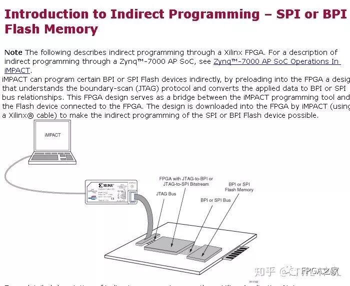
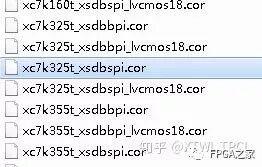
Indirect programming first configures the FPGA as a Flash read/write controller, and then uses this controller to read/write the Flash, so the configuration process shows that the FPGA is successfully loaded first, and then subsequent Flash operations are performed. In Xilinx, this Flash read/write controller is stored in the installation path of the tool. In ISE, it is referred to as a cor file.
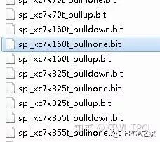
Vivado directly saves the bit file and provides three modes, differing in whether unused pins are pulled up, pulled down, or left in a high impedance state.
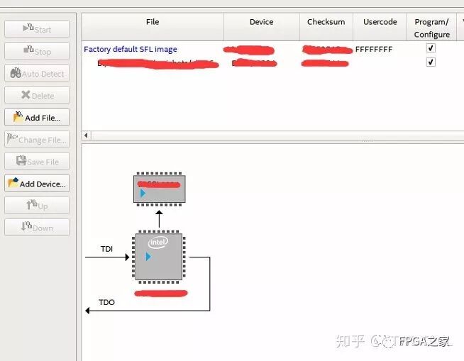
Intel (Altera) uses the file extension jic for this mode, which stands for JTAG Indirect Configuration File. The principle is exactly the same as the description for Xilinx above. In the Quartus Programmer interface, after adding a jic file, there is a Factory default SFL image, which is the image that configures the FPGA as a Flash controller.
When programming Flash, pay attention to the messages printed in the console, as you can see that the Flash is only controlled for read/write after the first successful configuration. Subsequent articles will analyze the specific operations on Xilinx and Intel (Altera) platforms.
Depending on the configuration, updates can also be divided into active and passive updates.
If it is a passive update, there is usually an actively initiating device in the configuration process, commonly an MCU. This makes the configuration process relatively easy, as the data transmission, storage, and reading are handled by the master device. The entire update process can be updated as required, and the FPGA can be reloaded at an appropriate time. The FPGA itself is almost completely isolated from the update process, making it easy to meet the requirements.
Active updates are relatively more complicated. First, the Flash may only have a data interface with the FPGA, indicating that the read/write operations on the Flash can only be initiated from the FPGA; secondly, since the FPGA needs to initiate the Flash update write, how the FPGA obtains the data is also a consideration. Referring to the description of the complete process of active configuration updating the Flash, it can be seen that the FPGA needs a data path (JTAG) to receive configuration data and implement a Flash read/write controller to read/write the Flash. After the Flash update is complete, the next configuration trigger (power cycling) will actively initiate the read operation from the Flash to load the configuration data and complete the configuration.
Now, you should have a preliminary understanding of remote updates.
If conditions permit, using an MCU as the main control device for remote updates will simplify the solution significantly. Moreover, software can be utilized for more operations (e.g., data verification). The usual reason for this choice is that there is already a master MCU in the system, which can simultaneously undertake the task of remote updates.
If the FPGA board uses an active configuration mode, since the read/write of the Flash can only be achieved through the FPGA, and directly updating the FPGA image via JTAG may not meet the requirements (for example, it is not feasible to configure via JTAG every time the power is cycled), then designing an active mode remote update solution becomes very important. At this point, even if there is an MCU or host computer in the system, since the Flash can only be controlled by the FPGA, the MCU/host computer mainly serves as a data communication channel to send FPGA configuration data, while the steps to update the Flash still need to be implemented by the FPGA.
It can be seen that if the update control is handed over to the MCU, the burden is significantly reduced. The requirements on the FPGA during the configuration process are minimal, and most of the work is completed by external devices (MCU), leaving little workload for the FPGA. Therefore, the focus of the discussion is on the more challenging active update solutions that require more work from the FPGA. Based on this, the current design requirements have become:
1. Utilize existing data channels to transmit data to the FPGA;
2. Write the update data into the Flash through the FPGA;
3. Ensure that the normal functionality of the FPGA is not affected during the Flash update process;
1. Utilize existing data channels to transmit data to the FPGA;
Since there are many options for data transmission, and each option is a significant topic, it will not be described in detail here. The recommended approach is to implement handshake control to write data into the Flash one by one. The design focus is on the interaction handshake and cross-clock domain between data transmission and Flash read/write.
Typically, the data transmission rate is higher than the Flash read/write rate, so using a buffer is advisable. On one hand, the storage space can easily overflow, and on the other hand, the frequency of update operations is not high. It is not cost-effective to reserve a large storage space for a low-frequency application. Therefore, using interaction handshake to handle the relatively slow update speed does not significantly impact the low-frequency Flash update operations, but the issue that arises is that cross-clock considerations need to be taken into account during the interaction.
2. Write the update data into the Flash through the FPGA
3. Ensure that the normal functionality of the FPGA is not affected during the Flash update process
These two requirements must be implemented by the FPGA, and the specific solution is that after the FPGA receives the data, it begins the read/write operations on the Flash, correctly writing the data into the Flash. Regarding this point, since it is related to specific FPGAs, there will be further analysis in subsequent articles targeting Xilinx and Intel (Altera) platforms.
Through a complete analysis, you should have a general understanding of what needs to be done for remote updates. Apart from the data path, the read/write control on the FPGA side is an inevitable requirement.

Want to learn about FPGAs? Here are example shares, ZYNQ design, follow our public account to explore.