Introduction The rise of domestic new materials is imminent, with a favorable cycle approaching. Emerging technology industries such as semiconductors and artificial intelligence are expected to become the focus of the chemical industry in 2024, bringing opportunities for new materials related to consumer electronics (OLED, VR/AR/MR), artificial intelligence (computing power-related), robotics (lightweighting), and semiconductors (wafer manufacturing and advanced packaging). At the same time, the transformation and iteration of materials in the new energy sector have never stopped: in photovoltaics, POE particles have yet to be domestically produced, boasting strong profitability and are expected to usher in several years of dividends; in lithium batteries, with the penetration of 800V fast charging, the profitability of conductive carbon black is expected to increase significantly.
1
OLED Materials
Medium size is the next “main battlefield” in the OLED industry, and Apple’s route switch may trigger industry transformation. Generally speaking, larger display panel sizes correspond to lower yield rates and higher costs. Compared to the mature process of LCD, OLED technology started later and is more difficult; currently, the mainstream production line for OLED is Generation 6, while LCD has evolved to Generation 10. Due to immature technology at the process end, OLED panels have mainly been used in small-sized mobile phones in the past. Currently, OLED penetration in smartphones is nearing maturity, with a penetration rate of 50%, while in the medium-sized panel field, the penetration rate is less than 2%, indicating significant room for growth. From a technical perspective, the yield rate for medium-sized panels in the display industry continues to improve, and with the rapid deployment of Generation 8.6 production lines for medium-sized production, the manufacturing costs per unit area for medium-sized OLED panels can be reduced by 48%, making medium-sized panel manufacturing more cost-effective. From the demand side, manufacturers such as Apple, Huawei, and Samsung are accelerating the switch of medium-sized products to OLED, effectively resonating with the technical advancements on the supply side, driving medium-sized penetration rates into a period of rapid growth.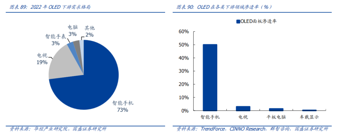 The switch in the Apple supply chain brings a huge demand increase. In 2023, global shipments of OLED tablet panels are expected to be about 3.5 million units, with a market penetration rate of about 1.4%, and the penetration rate for laptops is about 1.9%. In 2024, as Apple’s iPad, MacBook, and other products gradually switch to OLED, along with high-end product line layouts for OLED technology by brands like Samsung, Huawei, and Honor, OLED penetration in the medium-sized field is expected to achieve rapid growth. According to Sigmaintell’s forecast, by 2024, the global penetration rate of OLED panels in tablets and laptops will rise to 3.6% and 5.7%, respectively, and by 2028, it is expected to reach 21.5% and 17.9%. Major panel manufacturers are actively laying out Generation 8.6 lines, aiming at the medium-sized market. The generation line for OLED corresponds mainly to product size, with higher generation lines facilitating the production of large-size screens, primarily determined by the fine cutting process in manufacturing. The mainstream Generation 6 line has advantages in producing small-sized mobile phones and folding screen products, while the best production line for medium-sized tablet manufacturing is the Generation 8.6 line. In April 2023, Samsung Display announced an investment of 4.1 trillion won to build the world’s first Generation 8.6 OLED production line for laptops and tablets. Domestic OLED panel leader BOE announced in November an investment of 63 billion yuan to build an 8.6 generation OLED production line in Chengdu, Sichuan. Meanwhile, downstream panel manufacturers such as LG and Tianma are rapidly laying out medium-sized production capacity, confirming the industry’s strong trends.
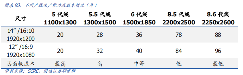
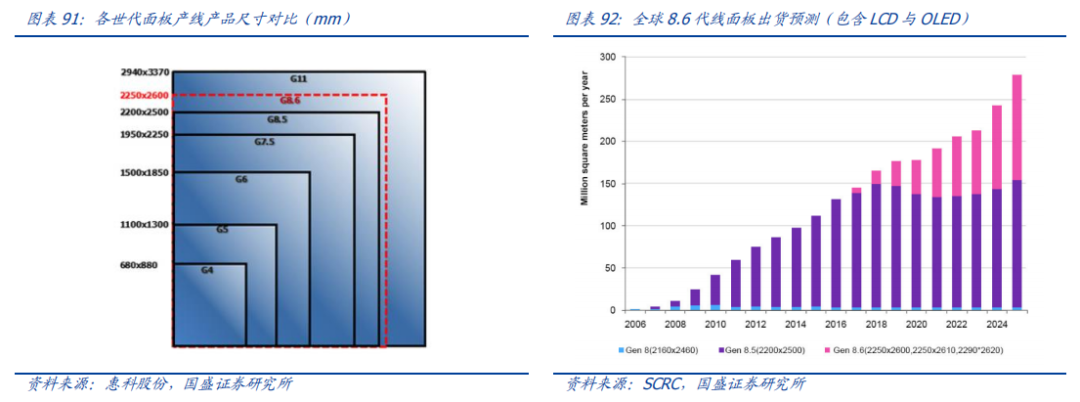 Generation 8.6 is the most economical medium-sized panel production line, with unit area costs decreasing by 48%. Compared to Generation 6, the Generation 8.6 line has better cutting utilization rates, making it more cost-effective for producing IT OLED panels of 10 inches or larger (2250x2600mm) compared to the Generation 6 line (1500x1850mm). From the perspective of unit production capacity, taking a 13.3-inch panel as an example, the Generation 8.6 line can increase production capacity to 96 units. In terms of manufacturing costs, the unit area manufacturing costs for medium-sized OLED panels produced on the Generation 8 line can be reduced by 48%, making medium-sized panel manufacturing more cost-effective.
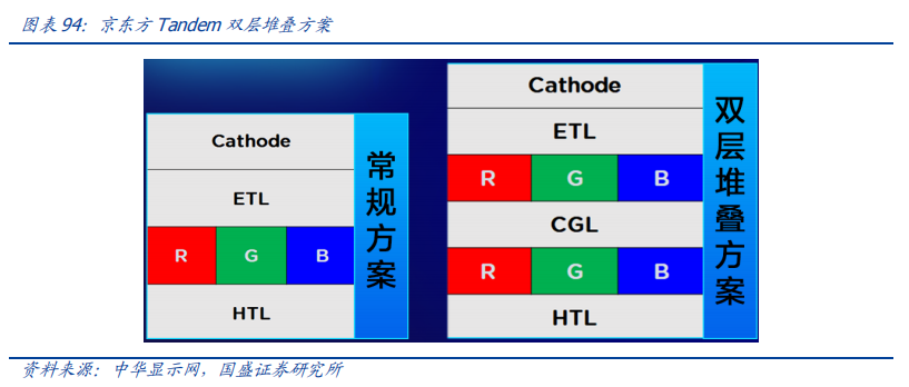
 Doubling area + dual-layer stacking, the new Generation 8.6 OLED production line opens up upstream material demand space. In terms of area, the Generation 8 IT OLED panel (2290 x 2620mm) is about 2.16 times larger than the Generation 6 panel (1500 x 1850mm); in terms of layers, BOE has introduced a Tandem dual-layer stacked OLED panel structure, which uses a double-layer light-emitting layer structure to achieve a 30% reduction in OLED power consumption and a 200%-300% increase in display device lifespan under the same brightness conditions. With the demand driven by the Generation 8 line and the Micro OLEDs in the MR field, it is expected that the dual-stacking structure will continue to penetrate into new OLED panels. Taking into account area, layers, and yield rates, it is expected that a single line of the Generation 8 line will increase upstream material usage to over four times that of the traditional Generation 6 line.
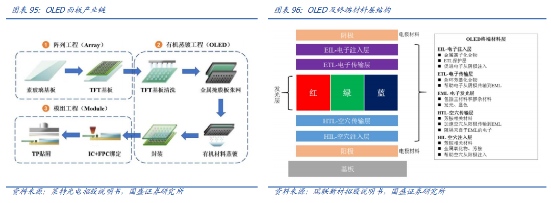
 OLED organic materials are applied in the organic vapor deposition process in panel manufacturing. The manufacturing of OLED display panels mainly includes three stages: array engineering, organic vapor deposition engineering, and module engineering. The array engineering mainly forms circuits through processes such as film formation, exposure, and etching on the substrate, while the organic vapor deposition engineering mainly combines organic light-emitting materials and electrode materials on the transistor circuit through vacuum vapor deposition, and the module engineering is mainly used to form complete module products. From the perspective of panel manufacturing stages, OLED organic materials are applied in the vapor deposition stage. OLED panels have a sandwich structure, and the terminal materials include the light-emitting layer and the common layer. OLED panels have a sandwich structure, specifically presenting OLED terminal materials distributed between two layers of electrode materials. When the electrodes are powered on, electrons injected from the cathode and holes injected from the anode combine in the light-emitting layer, simultaneously releasing energy in the form of light. The light-emitting layer achieves full-color display through independent light emission of red, blue, and green primary colors at different pixel points. The structure of OLED panels mainly includes electrode materials, substrate materials, and terminal materials: 1) Electrode materials: mainly metals and their oxides; 2) Substrate materials: mainly ITO glass or optical films; 3) OLED terminal materials: mainly divided into light-emitting layer (EML) and common layer, where the common layer includes electron injection layer (EIL), electron transport layer (ETL), hole transport layer (HTL), hole injection layer (HIL), etc. From the vapor deposition steps, the introduction order of various OLED organic materials is the hole injection layer, hole transport layer (forming a hole channel at this time), light-emitting layer (one main layer + doped material, one functional material), electron transport layer, electron injection layer (forming an electron channel), and cathode.
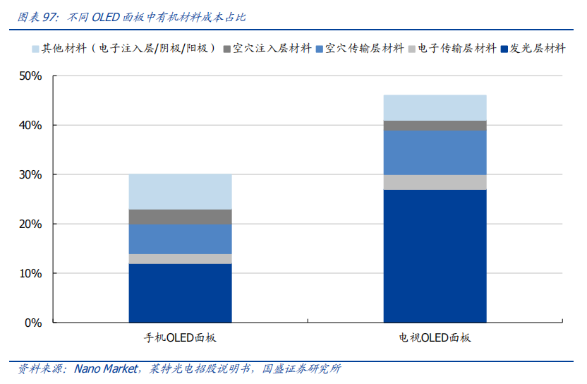
 Organic materials are the core cost source and the highest barrier stage in OLED panels, with a higher cost share in large-size panels. OLED organic materials are the core components in the manufacturing of OLED panels and are also one of the areas in the OLED supply chain with the highest technical barriers. Since OLED panels replace the optical films, polarizers, backlights, and liquid crystals in LCD panels with OLED terminal material layers, the cost share of OLED materials in the entire panel manufacturing is far greater than that of LCD. Specifically, organic materials account for about 30% of the cost in OLED mobile phone panels, while organic materials account for as much as 46% in OLED TV panels.
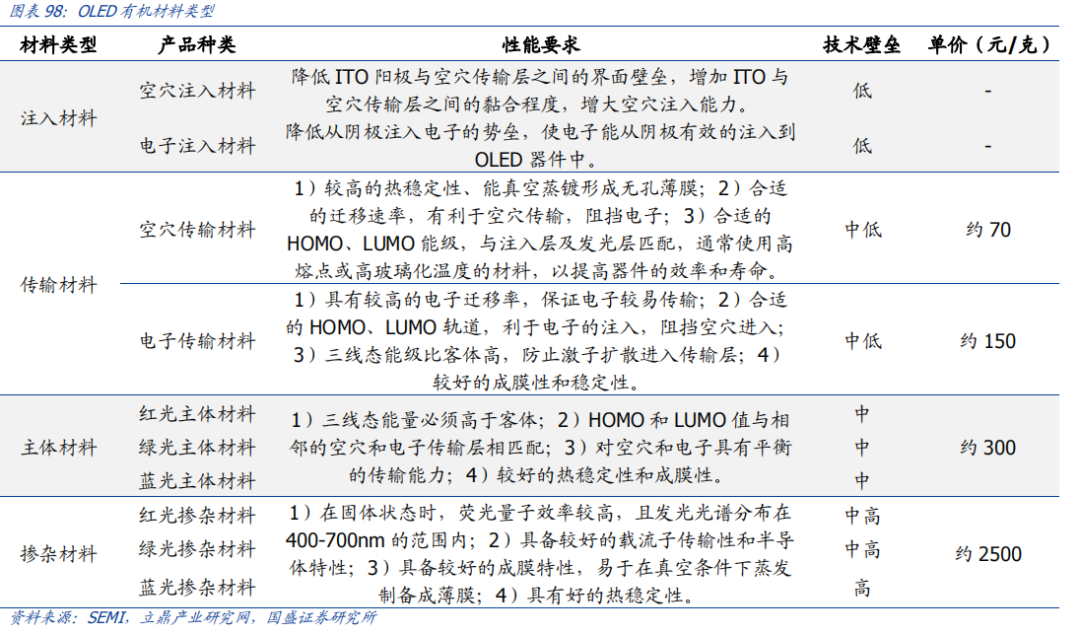
 Light-emitting layer materials are the core link of OLED terminal materials, characterized by high technical barriers and complex compositions. OLED terminal materials can be divided into 6 layers and 14 categories of materials, where light-emitting layer materials are the core part, mainly consisting of dopant materials, light-emitting host materials, and light-emitting functional materials, with the three types of light-emitting layer materials working together with the common layer materials to ensure that the device can stably and efficiently present good light-emitting effects.
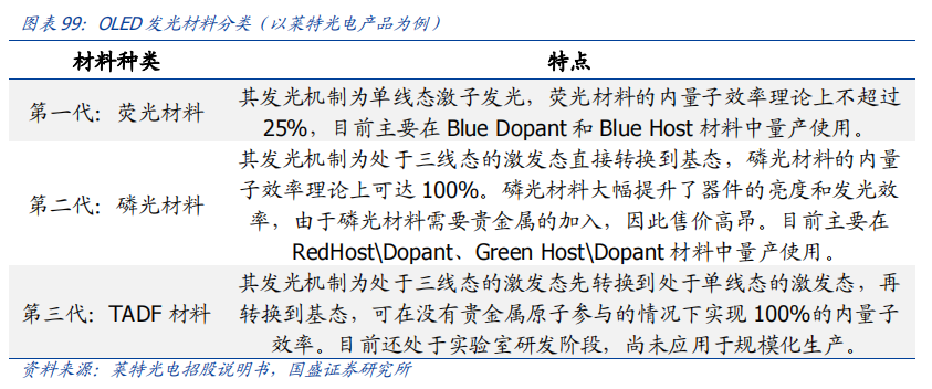
 From the perspective of light emission methods: OLED light-emitting materials mainly include three types: fluorescence, phosphorescence, and TADF: ✓ Fluorescent materials: Fluorescent emission is the first generation of light-emitting technology, mainly represented by green fluorescent materials such as tris(8-hydroxyquinoline) aluminum (Alq3). The fluorescence emission mechanism is an asymmetric rotation of singlet excitons, with low material costs but a light-emitting efficiency of only 25%; ✓ Phosphorescent materials: Phosphorescent emission is the second generation of light-emitting technology, capable of achieving emission under both singlet and triplet exciton rotation modes, with a theoretical light-emitting efficiency of up to 100%. However, the lifespan of blue phosphorescent materials under 95% of initial brightness does not exceed 1000 hours, which limits material applications. On the other hand, the precious metals (such as iridium, platinum, etc.) in metal complex phosphorescent materials are scarce and expensive, which also restricts the application of phosphorescence; ✓ TADF materials: The third generation of light-emitting technology TADF (thermally activated delayed fluorescence materials) can achieve 100% internal quantum efficiency without the participation of precious metal atoms, ensuring similar light-emitting performance to phosphorescent materials while achieving low-cost and efficient OLED technology applications. However, due to high technical barriers, it has not yet been commercialized.
 The global market for OLED terminal materials is nearly $2 billion, with the front-end material volume approximately 28% of the terminal material. Organic materials are the core cost source of OLED panels, in terms of terminal materials: in 2023, the global market size for OLED terminal materials is approximately $1.88 billion. According to TrendForce, it is expected that by 2025, the OLED organic materials market will reach $3 billion. Since the sales of OLED organic materials correspond to the sublimated finished materials, the above market size mainly refers to terminal materials. In terms of front-end materials: according to DSCC data, in 2019, the global market size for OLED front-end materials (intermediates + sublimation materials) was approximately $1.786 billion, accounting for about 28% of the OLED terminal materials market (calculated based on the 2019 market of $927 million).
  In terms of emission colors: red and green light mainly use second-generation phosphorescent materials, while blue light mainly uses first-generation fluorescent materials. OLED panels achieve display through the independent light emission of red, blue, and green primary colors at each pixel point, with the organic emission colors primarily being red, blue, and green. Among these, second-generation phosphorescent materials have penetrated in the red and green light fields, while using second-generation phosphorescent materials in blue light leads to faster attenuation, thus blue light currently predominantly uses first-generation fluorescent materials.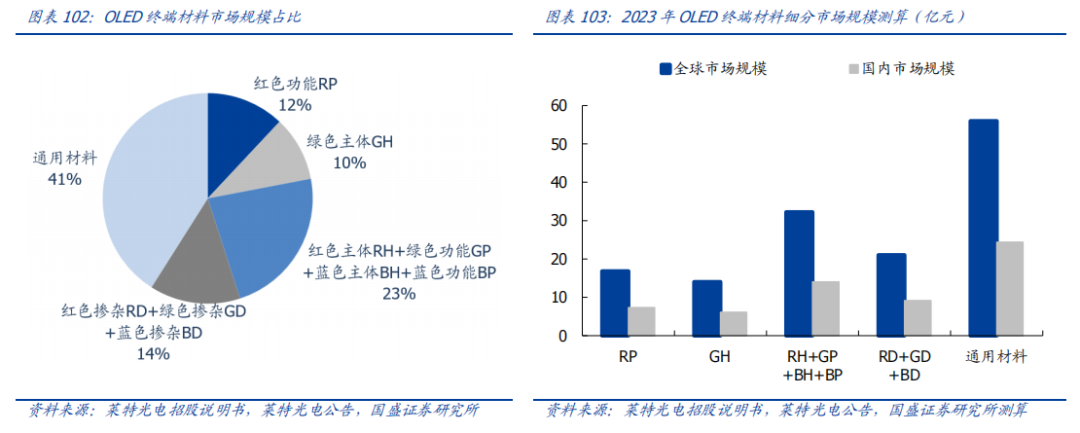
2
Upstream Materials for AR/MR/VR
Single machine value breakdown: silicon-based OLED costs account for as high as 46%. According to Wellsenn XR, the BOM cost of Apple’s MR headset is approximately $1509, with the cost of a single 1.3-inch silicon-based OLED internal screen being about $350, and the usage of 2 pieces corresponds to a cost of about $700, accounting for as much as 46% of the total cost of the MR headset. Other components with costs exceeding $50 include: M2 chip ($120), image processing chip ($60), pancake 3P optical module ($60), and structural components ($120). We focus on the upstream chemical materials of core components in Apple’s MR, mainly including silicon-based OLED materials and pancake optical module materials.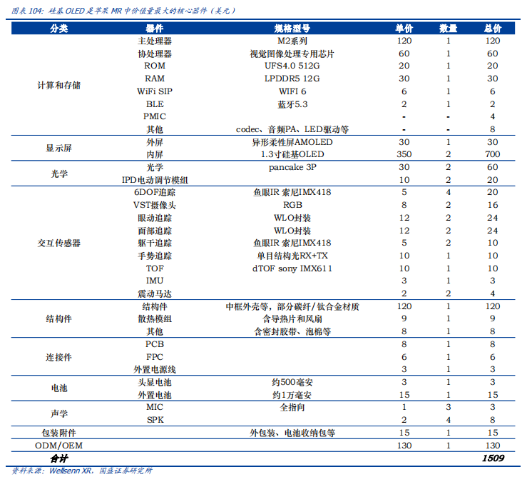 2.1. Silicon-based OLED substrates are expected to become the core device with the highest value. As downstream requirements for optical performance and lightweighting increase, the selection of XR screens has gone through three mainstream stages: OLED, Fast-LCD, and silicon-based OLED. Apple’s choice of the latest silicon-based OLED route establishes the industry trend.
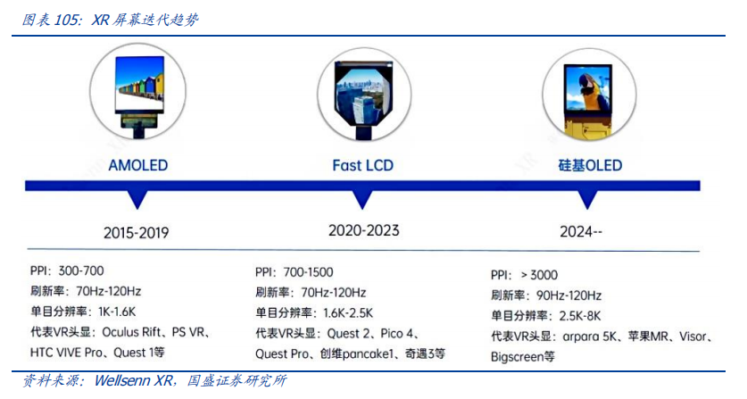 Increasing pixel density is the core of XR display. Unlike mobile phones and computers, XR is a near-eye display method, thus requiring higher screen resolution. The resolution is influenced by both screen size and pixel density, where small-screen devices require higher pixel density to achieve the same resolution as larger-screen devices, making the enhancement of panel pixel density the core of XR technology. Currently, Fast-LCD is the industry mainstream display route, but Fast-LCD’s pixel alternating arrangement easily reveals obvious horizontal or vertical lines in the picture, known as the moiré effect, greatly affecting immersion. However, due to the characteristics of the materials themselves, the moiré effect of Fast-LCD is difficult to eliminate; even with a single-eye resolution of 2.5K, it still cannot mask the presence of the moiré. Meanwhile, Fast-LCD has disadvantages in terms of screen weight and volume, indicating poor lightweight properties, which are expected to be gradually phased out by the industry. PPI is the core indicator of pixel density, and silicon-based OLED can reach above 3000. PPI (Pixels Per Inch) refers to the unit of pixel density, indicating the number of pixels along the diagonal per inch. The higher the PPI value, the higher the density at which the display can show images. For near-eye displays, to eliminate the moiré effect, VR devices need to achieve at least 60 PPD resolution, corresponding to a PPI of 3000-4000. Currently, the highest PPI for mass-produced ordinary OLED is only 800, while Fast LCD’s mass production PPI is about 1500, and silicon-based OLED can reach a maximum PPI of 4000. Silicon-based OLED can achieve single-eye 4K and dual-eye 8K levels (PPI 4000, using a 1.4-inch screen).
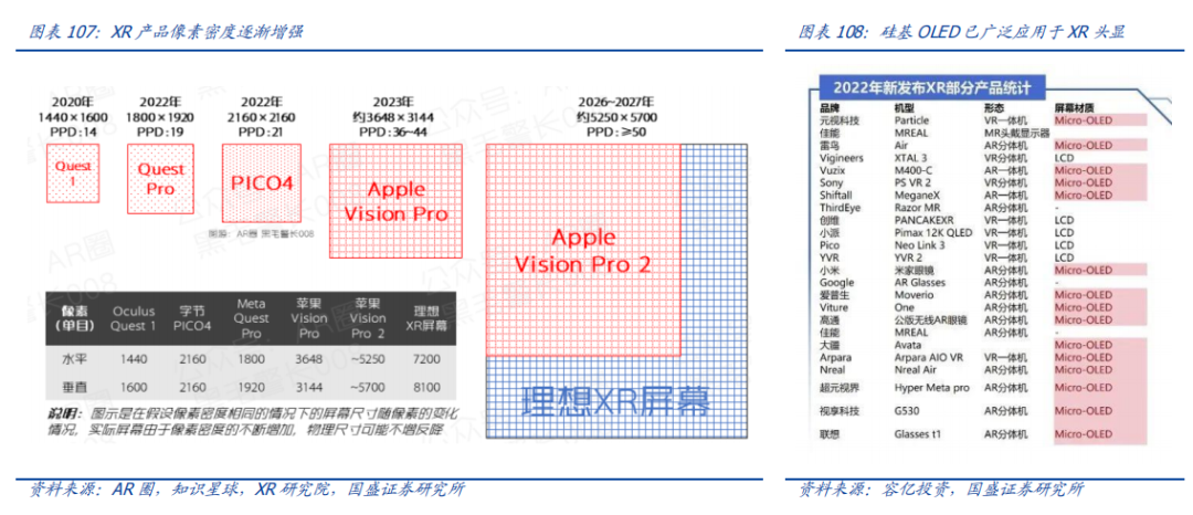
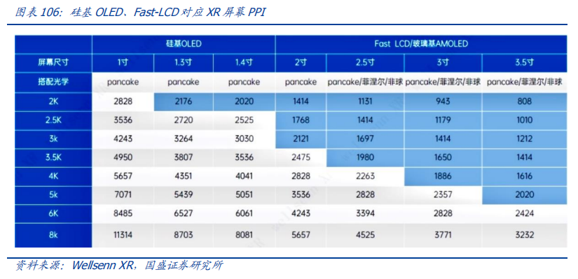 Silicon-based OLED was first applied in military fields and is currently the preferred display route for new XR. Silicon-based OLED (MicroOLED) was first used in military applications, including targeting observation systems, helmet systems, and combat simulation training systems, and has rapidly penetrated into civilian fields such as XR devices and medical equipment. Silicon-based OLED directly mounts micro-displays on wafers, using single-crystal silicon wafers as backplanes, allowing displays to achieve high brightness, high resolution, high refresh rates, high contrast, low power consumption, and small volume, making it the best choice for near-eye displays. Currently, manufacturers such as Apple, Meta, Thunderbird, and DJI are using Micro-OLED micro-display solutions, and the industry trend is gradually clarifying.
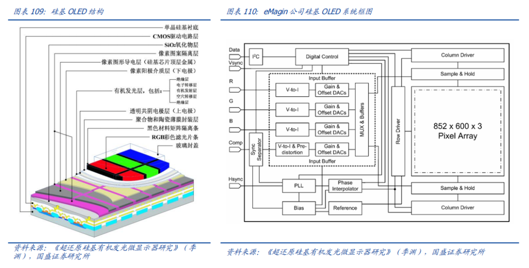
 Silicon-based Micro-OLED is a new generation display technology that combines advanced CMOS semiconductor processes with OLED processes. In traditional OLED, the light-emitting layer is protected by a sealed cavity formed by a cover, sealing adhesive, and glass substrate, while silicon-based OLED uses single-crystal silicon as an integrated driving backplane, with the main process being to fabricate organic light-emitting devices on single-crystal silicon integrated circuit chips that have integrated video signal processing and pixel driving arrays, equipping each pixel with controllable output current CMOS transistors and charge storage capacitors, thus eliminating the need for additional driver ICs in LCD or OLED. From the perspective of structure and corresponding processes, the main differences between silicon-based OLED and traditional OLED lie in the substrate and driving circuit, specifically: Substrate (wafer): Depending on the substrate, it can be divided into glass substrates, silicon substrates, and flexible substrates. Due to differences in PPI pixel circuits, micro-sized Micro-OLED displays generally use silicon substrates, while medium, small, and large-sized OLEDs usually use glass or flexible substrates. Compared to the glass substrates used in traditional OLED, single-crystal silicon backplanes have higher carrier mobility, allowing silicon-based OLED to fabricate smaller pixel sizes, achieving miniaturization and refinement of display pixels; Driving circuit: Micro-OLED uses single-crystal silicon semiconductors as substrates, integrating millions of transistors to form CMOS dynamic circuits; Oxide layer: The top layer of ordinary CMOS circuits is generally an oxide passivation layer, while the top layer of silicon-based micro-displays is a conductive layer for pixel patterns; Similar layers to traditional OLED: From bottom to top, they are the lower electrode, isolation layer, organic light-emitting layer, and upper electrode (used to connect all pixels’ cathodes), with a structure similar to traditional OLED; Packaging layer: Sealed with a glass cover.
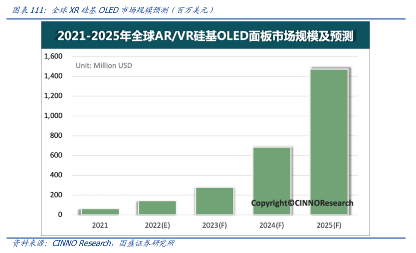
 The XR silicon-based OLED market is expected to reach billions of dollars in the long term, with vast growth potential. According to CINNO Research, the global market size for AR/VR silicon-based OLED display panels was $64 million in 2021, and it is expected to grow significantly to $1.47 billion by 2025, with a compound annual growth rate of about 119%. In the long term, based on Apple’s cost breakdown of $700 per unit for MR, it is estimated that the market space for silicon-based OLED will be $2.1 billion, $4.2 billion, $7 billion, and $10.5 billion for shipments of 3 million, 6 million, 10 million, and 15 million MR devices, respectively.
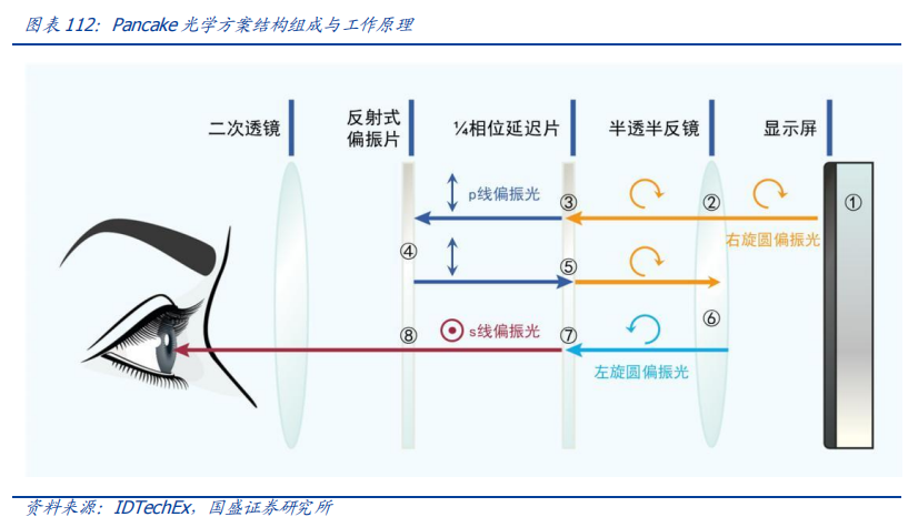
 2.2. Pancake drives high demand for COC. Pancake is a definitive technology route for VR displays, with Apple adopting a 3P solution that increases the number of lenses to 6. Currently, the core products of leading VR manufacturers worldwide have generally adopted Pancake optical modules. The mainstream Pancake solutions include 2P and 3P, corresponding to 2-piece and 3-piece lenses. Currently, Apple uses the latest 3P Pancake structure, which has higher image pixel quality and lower color difference compared to traditional 2P, while improving overall imaging performance and lightweight characteristics. Pancake accounts for a high proportion of XR headset costs and is an important component affecting imaging performance. Pancake involves a complex multi-layer optical structure. As the third generation of VR imaging routes, Pancake has advantages such as lightweight, high imaging quality, and adjustable refraction. The optical structure of Pancake consists of half-transparent and half-reflective BS, polarizers, reflective polarization films RP, and 1/4 phase delay plates QWP. Its optical principle is as follows: 1) The right-handed circularly polarized light emitted from the display screen passes through the BS beam splitter (half-transparent and half-reflective film); 2) The right-handed circularly polarized light passes through the 1/4 phase delay plate and becomes P-line polarized light parallel to the incident plane, and is reflected by the reflective polarization film; 3) It passes through the 1/4 phase delay plate a second time; 4) After being reflected by the BS beam splitter, the right-handed circularly polarized light becomes left-handed circularly polarized light; 5) It passes through the 1/4 phase delay plate a third time, turning left-handed polarized light into S-line polarized light perpendicular to the vibration direction; 6) The S-line polarized light passes through the reflective polarization film and finally reaches the human eye.
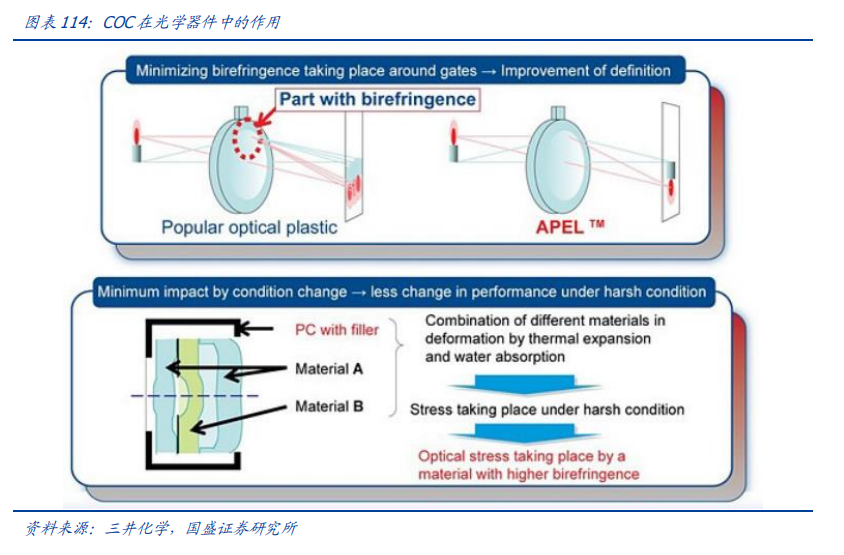
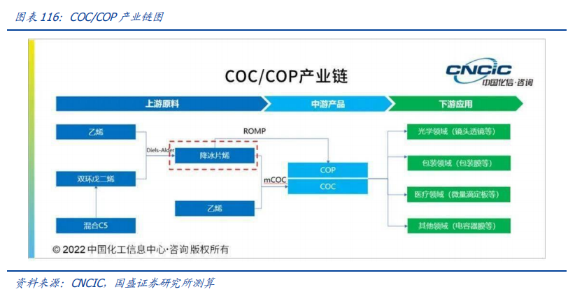
 COC/COP performance is excellent, with a wide range of applications. The main raw materials for COC/COP are ethylene and norbornene, where norbornene is usually prepared from dicyclopentadiene (DCPD) or cyclopentadiene (CPD) through a Diels-Alder reaction with ethylene. Classified by polymerization routes, COC is formed by the copolymerization of olefin and cyclic olefin monomers, while COP is formed by the polymerization of cyclic olefin monomers. COC has low density, high strength, good dimensional stability, high refractive index, excellent UV/visible light transmittance, good moisture barrier properties, and good heat and chemical resistance, making it widely used in optical materials, medical hygiene packaging materials, food packaging materials, and electrical materials. COC/COP is the preferred resin material in high-end optical fields. In the field of optical lenses, mainstream optical resins include PMMA and COC/COP, with COC/COP outperforming PMMA on the performance front, making it more suitable for high-end optical devices. Specifically: 1) Low hygroscopicity: PMMA has the disadvantage of high moisture absorption, while COC/COP has low moisture absorption, overcoming PMMA’s performance weaknesses; 2) High lightweighting: COC/COP has a density of less than half that of ordinary glass and is not easily broken, suitable for applications requiring high weight, durability, and cost for optical components; 3) Strong thermal performance: COC/COP can withstand high temperatures above 100°C, and can operate for long periods in extremely cold conditions, with very low moisture absorption rates and excellent creep resistance at different temperatures; 4) Strong wear resistance: COC is the most wear-resistant optical material, effectively preventing damage when used as a lens; 5) Strong self-lubrication: COC has excellent self-lubricating properties, suitable for lens assembly processes in mobile phones; 6) Strong plasticity: COP has a refractive index similar to glass and strong plasticity; 7) Low birefringence: COP’s low birefringence is widely used in display panels for dimming. Based on comprehensive performance advantages, COC/COP is widely used in smartphone lenses, security lenses, automotive lenses, polarizing film protective films, display screen films, back-projection TV photosensitive components, and projector photosensitive components. At the same time, COC/COP, as AR/VR optical lenses, can effectively achieve lightweighting of AR/VR devices while providing excellent optical performance.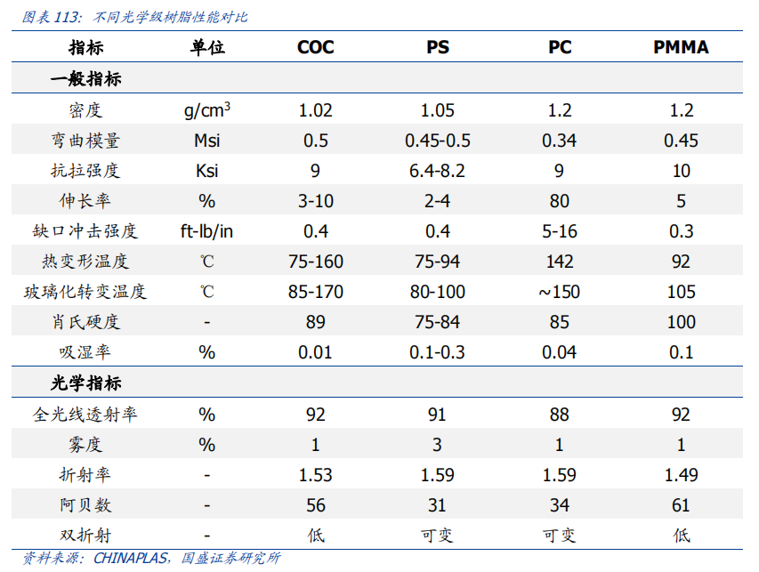
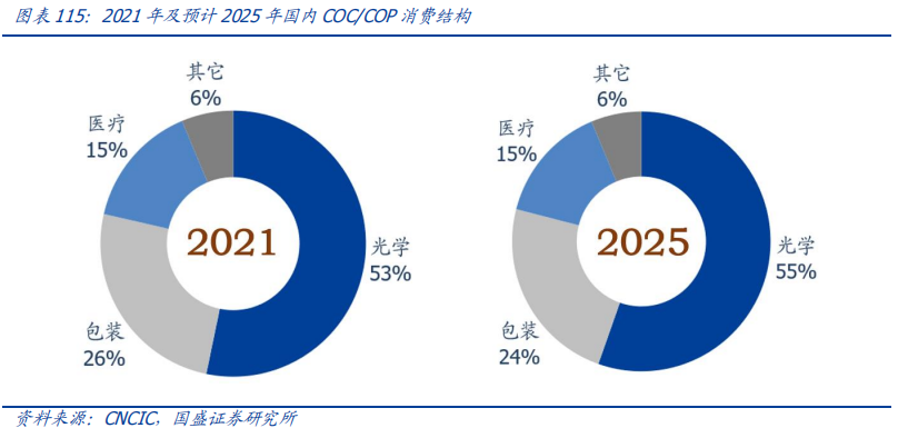
 By 2025, the domestic market for COC/COP is expected to reach 10 billion yuan, with optics being the largest application field. According to the China Chemical Information Center, in 2021, China’s consumption of COC/COP was about 21,000 tons, making it the major consumption market for COC/COP globally. In 2021, the consumption of COC/COP in the optical field was about 11,000 tons, accounting for 53.2%, while the consumption in packaging and medical fields was 5,200 and 3,100 tons, accounting for 25.3% and 15.1%, respectively. It is expected that by 2025, China’s consumption of COC/COP will increase to 29,000 tons, with the demand in the optical field rising to 16,100 tons, accounting for 55.4%. Based on optical-grade prices of 500,000 yuan/ton and other grades at 150,000 yuan/ton, it is estimated that the domestic market for COC/COP will increase from 7 billion yuan in 2021 to 10.7 billion yuan by 2025. The two major technical barriers are high, making the industrialization of COC/COP extremely challenging. The upstream of COC/COP mainly consists of cyclic dienes (primarily dicyclopentadiene or cyclopentadiene) and low-carbon α-olefins (mainly ethylene), where dicyclopentadiene (cyclopentadiene) and ethylene generate the key monomer norbornene through D-A addition reactions. Additionally, norbornene can also serve as an intermediate to undergo D-A addition reactions with cyclopentadiene and other cyclic olefins to generate tetracyclic dodecene and other polycyclic olefin monomers. Polycyclic olefin monomers can be homopolymerized through the ROMP (ring-opening metathesis polymerization) process or copolymerized with norbornene through a metallocene-catalyzed addition process (mCOC). The refractive index of COC films increases linearly with the increase in norbornene content, and samples with a uniform distribution of copolymer composition exhibit better transparency. Adding long-chain polar α-olefins can improve the refractive index and hydrophilicity of the film. Currently, Japan’s Riwon and Japan Synthetic Rubber use the ROMP process, while Japan’s Toray Plastics and Mitsui Chemicals use the mCOC process.
 COC/COP is mainly monopolized by Japanese companies, while domestic manufacturers are accelerating their layout. Due to high technical barriers in the synthesis of norbornene monomers, metallocene catalysts, and polymerization processes, large-scale production companies are currently concentrated in Japan. Specifically: COP: Due to the challenges in controlling temperature and material performance in the ROMP process, only Riwon currently has industrial production capabilities (with a production capacity of 42,000 tons in 2021), and its products are widely used in optics, food, and medical fields; COC: Overseas manufacturers include Toray Plastics, JSR, and Mitsui Chemicals, with production capacities of 30,000, 5,000, and 6,000 tons in 2021, respectively, totaling 41,000 tons, with a combined capacity of COC and COP of 83,000 tons. Optical-grade COC/COP requires stricter standards than ordinary grade products in TMA, haze, and other indicators; only a few players like Mitsui Chemicals and Riwon have the capability to produce high-end optical-grade products. Currently, domestic companies such as Acolyte, Tuoxian Technology, Baismei, Luhua Hongjin, Wanhua Chemical, and Kingfa Technology are accelerating the layout of COC and upstream norbornene production capacity, with breakthroughs in domestic production expected.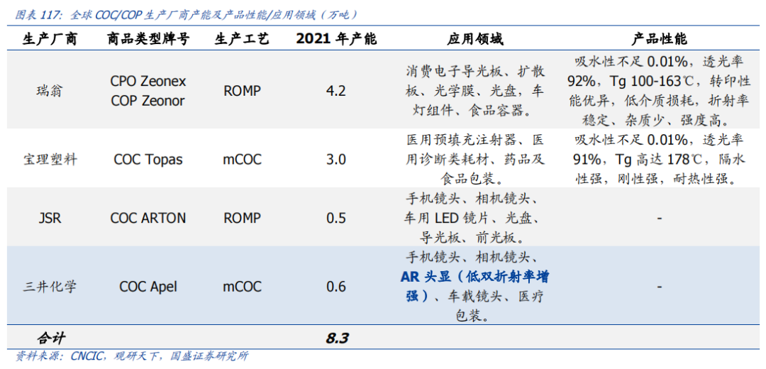
3
Materials for Robotics and Artificial Intelligence
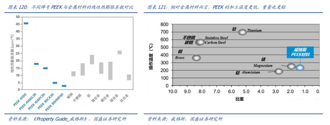
3.1. PEEK Materials PEEK (Polyether Ether Ketone) is the “all-rounder” among materials, exhibiting excellent performance that other plastics or metals cannot match. As a member of PAEK (Polyarylether Ketone), the aromatics and ketones in PEEK provide rigidity and chemical inertness, giving PEEK good mechanical properties, high melting points, and corrosion resistance, while the ether bonds somewhat enhance the material’s flexibility. From a molecular structure perspective, PEEK’s molecular chain is highly organized, providing some crystallinity, which in turn offers wear resistance, creep resistance, fatigue resistance, and chemical resistance. Although PEEK’s individual performance may not be the best, its combination of high-temperature resistance, flame retardance, recyclability, wear resistance, flexible processing, and corrosion resistance makes it a standout material with unique comprehensive performance.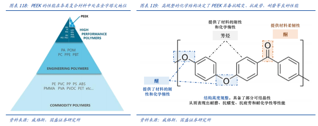 Compared to metal materials, PEEK’s advantages in thermal stability and low density make it more suitable as a lightweight material in automotive and aerospace fields. At temperatures below the glass transition temperature, PEEK composites even exhibit better thermal expansion coefficients than metals, with good dimensional stability, and higher stability at both high and low temperatures. Additionally, PEEK’s density is lower than that of magnesium and aluminum, and even when carbon fibers are added to the matrix, it does not significantly increase its density. Coupled with PEEK’s high specific strength, it can greatly reduce the material’s own weight while meeting strength requirements, making it a solution for achieving lightweighting. In the medical field, PEEK can replace metals such as zirconium and titanium for human bones, and in the automotive field, it can be used to manufacture engine covers, bearings, clutch gears, and other components.
 PEEK is recognized as one of the best-performing thermoplastics in the world, with various performance indicators leading compared to other composite materials.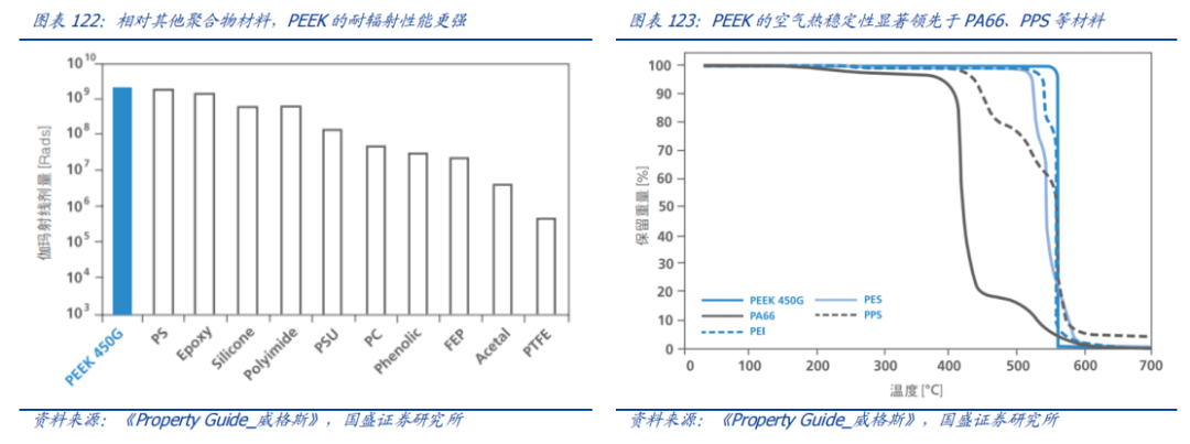
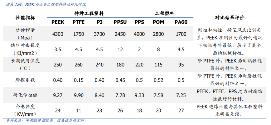 After domestic production, the application prospects for PEEK materials are promising. As a thermoplastic material, PEEK can be processed using traditional thermoplastic processing equipment for injection molding, compression molding, and extrusion, making it widely applicable in industries such as petrochemicals, automotive engines, aerospace, and medical fields. In the future, PEEK materials are expected to have promising applications in the 800V fast charging field and in robotics.
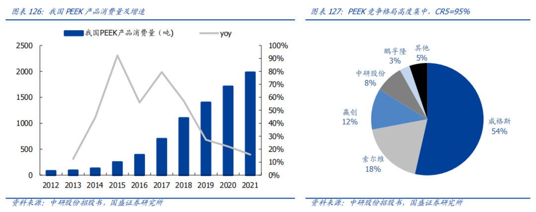
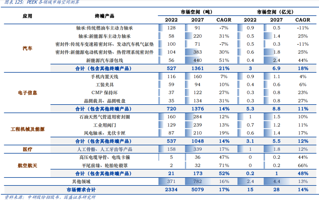 The competitive landscape for PEEK materials is excellent. The global supply concentration of PEEK is very high, with the top three overseas giants accounting for 84% of the market share, and this is also the case in China. In 2021, China’s annual consumption of PEEK products was about 2000 tons, most of which were still supplied by overseas giants such as Victrex, Solvay, and Evonik. Currently, precision machining is one of the main downstream applications for PEEK, and in recent years, domestic companies such as Ningbo Zheneng, Jiangsu Junhua, Nanjing Shousu, Longyue Environmental Protection, and Shenzhen Enxinlong have emerged as special engineering plastic manufacturers. There is a demand from downstream customers to find domestic suppliers to reduce material costs, and we believe that in the future, the share of domestic PEEK materials will continue to concentrate in companies of a certain scale in China.
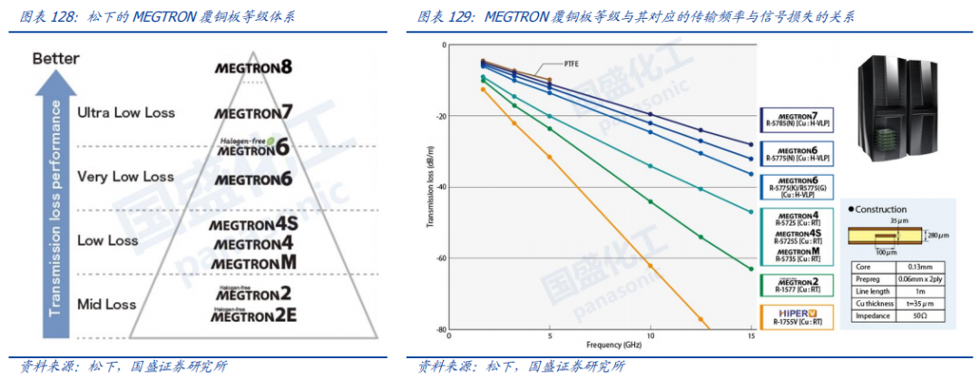
 3.2. High-Frequency and High-Speed Resins Driven by emerging technology industries such as AI servers and smart automotive radars, demand for high-frequency and high-speed copper-clad laminates is expected to grow significantly. High-frequency and high-speed copper-clad laminates, which have low signal transmission loss as the most important characteristic, refer to CCLs (Copper-Clad Laminates) for RF/microwave circuits (referred to as “high-frequency CCL”) and CCLs for high-speed digital circuits (referred to as “high-speed CCL”). High-frequency and high-speed copper-clad laminates have high requirements for the dielectric constant (Dk) and dielectric loss (Df) of their filled resins. Among these, high-frequency products are very sensitive to changes in the dielectric constant (Dk), while high-speed materials have higher requirements for dielectric loss (Df) and are relatively insensitive to dielectric constant (Dk). The iteration of technology industries drives the upgrading of high-frequency and high-speed copper-clad laminates. Panasonic’s launched high-speed product series MEGTRON (M2-M8) has become a benchmark product in the industry, with higher levels corresponding to lower dielectric loss and higher transmission rates. Based on different electrical grades, resin materials and terminal applications can be classified, with AI servers mainly using M6-level and above ultra-low loss copper-clad laminates, and smart automotive radars mainly using M4-level low-loss copper-clad laminates. We believe that the growth in emerging technology applications such as AI servers and smart automotive radars is expected to drive demand for high-frequency and high-speed copper-clad laminates with superior dielectric performance.
 Driven by emerging technology industries, resins such as PPO, BMI, reactive esters, and hydrocarbon resins are expected to enter a high prosperity phase: ✓ PPO: Polyphenylene oxide resin (PPO) is a type of thermoplastic resin with excellent dielectric properties, thermal stability, dimensional stability, and low water absorption. After modification, it is widely used in high-frequency and high-speed copper-clad laminates, mainly as high-speed copper-clad laminates; ✓ BMI: Bismaleimide resin (BMI) is a thermosetting resin with bismaleimide as the active end group, possessing excellent heat resistance, thermal oxidation resistance, flame retardance, as well as high bending strength, modulus, dimensional stability, good electrical insulation, and wave transmission properties. It is widely used in high Tg substrates, IC packaging substrates, and M6-level and above requirements, as well as in aerospace, aviation, and military equipment in high-end fields; ✓ Reactive esters: Reactive ester curing agents contain two or more highly active ester groups that can react with epoxy resins, forming a network structure without secondary alcohol hydroxyl groups, resulting in low dielectric loss and water absorption, suitable for high-speed copper-clad laminates; ✓ Hydrocarbon resins: Hydrocarbon resins (PCH) are thermoplastic polymers formed by the polymerization of unsaturated hydrocarbons. Due to their lower molecular polarity and crosslink density, hydrocarbon resins exhibit excellent low dielectric performance, typically used in high-frequency and high-speed copper-clad laminates along with PPO and BMI for AI and 5G applications.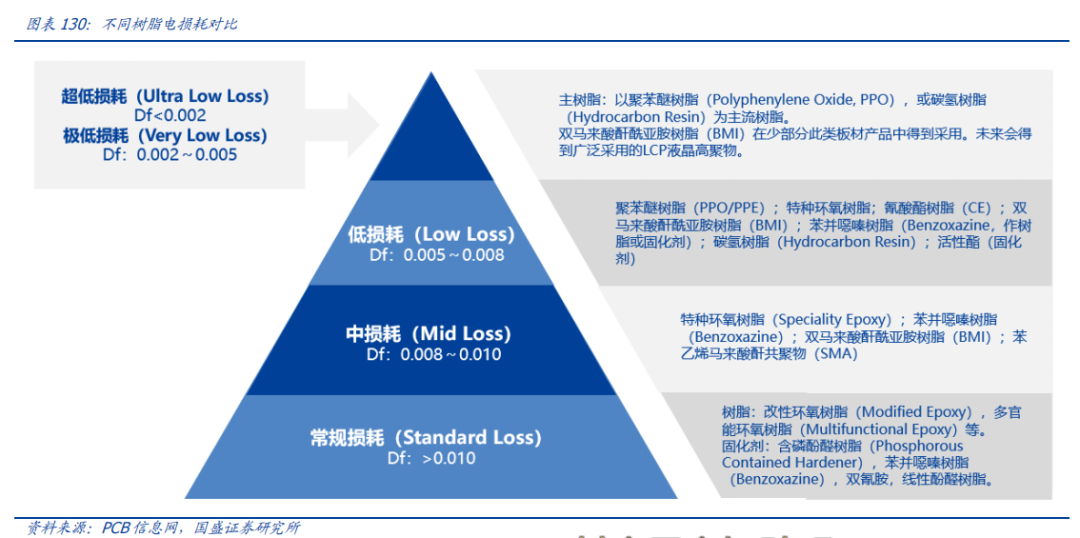
4
New Energy Major Products with Excellent Patterns
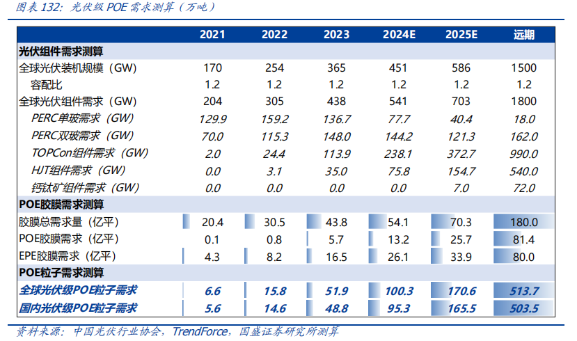
4.1. POE POE adhesive film is the mainstream packaging material for N-type batteries and perovskite batteries, with new technology routes opening up demand for POE particles. The barrier properties, strong PID resistance, and absence of acetic acid in POE products give them inherent advantages in TOPCon and heterojunction batteries, making them the primary packaging adhesive film for N-type batteries, where TOPCon batteries use POE or EPE adhesive films, and HJT batteries use POE adhesive films. Looking ahead, perovskites are currently recognized as the next mainstream battery route after N-type batteries, with both upper and lower layer packaging materials using POE adhesive films. Driven by the iteration of new technology routes in photovoltaic batteries (modules), POE demand is expected to experience nonlinear growth.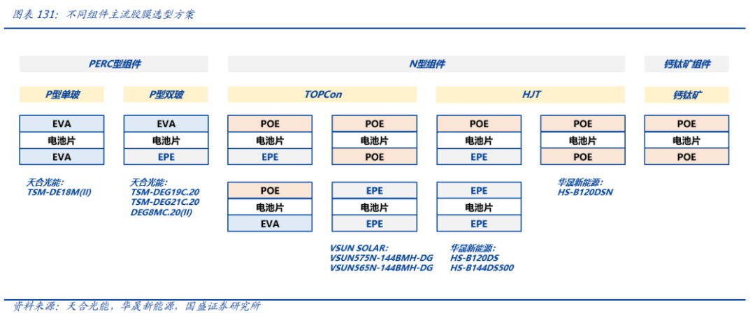 Based on our estimates, POE adhesive films are rapidly penetrating the market, with global demand for photovoltaic-grade POE particles expected to reach 1.7 million tons by 2025. In the long term, as photovoltaics enter the TW era, China’s demand for POE is expected to exceed 5 million tons. With the continuous iteration of battery routes, POE, as the mainstream packaging adhesive film material for TOPCon, HJT, and perovskite, has enormous penetration potential, and as photovoltaics enter the TW era, global demand for POE/EPE adhesive films is expected to exceed 10 billion square meters, with particle demand expected to exceed 5 million tons.
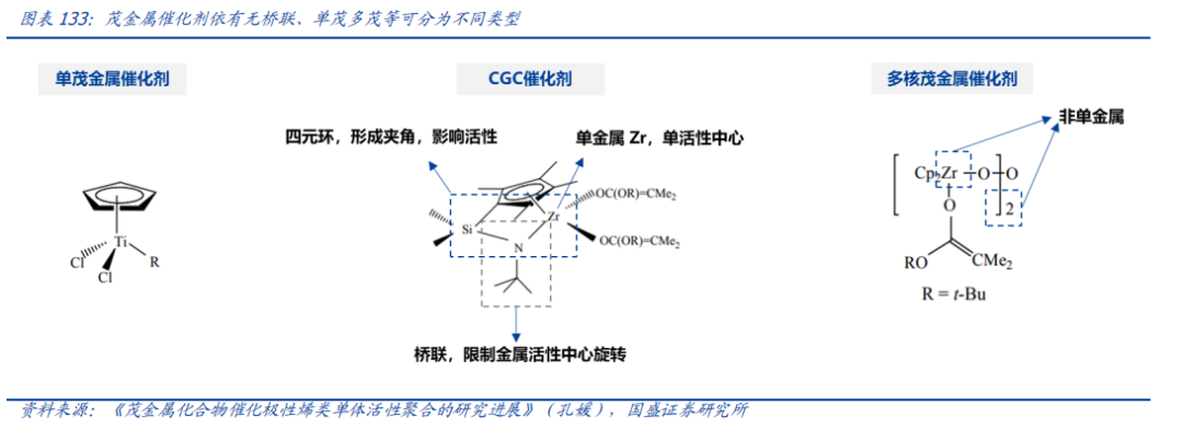
 Constrained geometry catalysts (CGC) are a typical choice for efficient synthesis of POE. Compared to traditional Z-N catalysts, CGC catalysts have strong controllability over the molecular weight of polymers, copolymer content, and the regularity of structures, enabling the production of high-performance POE with narrow molecular weight distribution and long-chain branching. CGC, as a bridged metallocene structure, was first applied by Dow in the Insite process in 1993. The “constrained” feature of this catalyst is reflected in its pseudo-quadrilateral structure of Cp-M (metal)-N-Si. The presence of the quadrilateral allows CGC to have two characteristics: 1) Variations in the angle between Cp-Ti-N affect electronic and spatial effects, altering catalyst activity; 2) Influenced by the bridging group, the rotation of the metal around the metallocene-nitrogen center is limited, allowing the active center to open only in one direction, favoring the insertion of long-chain copolymer monomers.
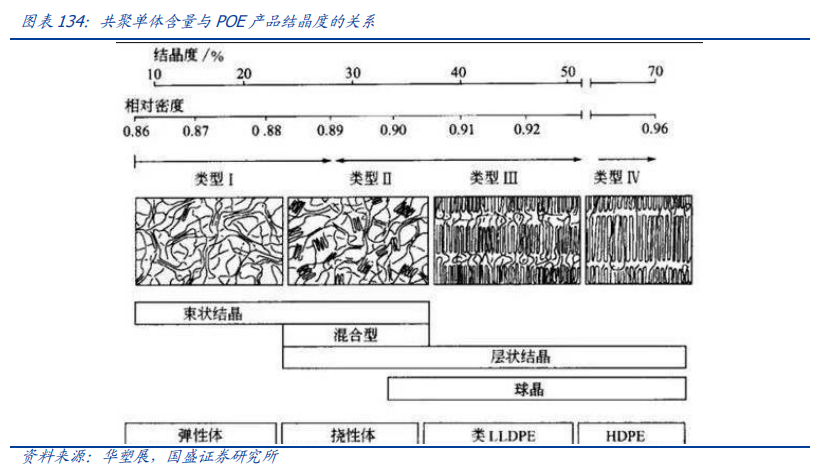
 The copolymerization of α-olefins can reduce the crystallinity of polyolefins, thereby meeting the high transparency requirements of photovoltaic adhesive films POE. In ordinary polyolefin products, the crystalline size is larger than the wavelength of incident visible light, leading to scattering of incident light and reducing product transparency. The essence of POE elastomers is branched polyethylene, where during the copolymerization process, long-chain α-olefins can form interpenetrating amorphous regions, breaking down the polyethylene chain segments into more numerous and shorter crystalline regions, improving product transparency while destroying larger crystallines. The more microcrystals formed as crosslinking points can increase the chain length, allowing POE to exhibit characteristics similar to plastics at high temperatures and rubber at room temperature. Coupled with the saturated structure of POE’s macromolecular chains, the product also exhibits excellent aging resistance and UV resistance.
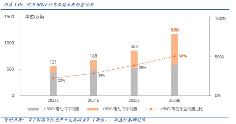
 4.2. Conductive Carbon Black By 2026, the share of high-voltage fast-charging vehicles is expected to reach 50%, with ownership rising to over 13 million vehicles. According to the plans released by major domestic car manufacturers for high-voltage fast-charging models of 800V and above, starting from 2023, high-end models that meet 3C and above high-voltage fast charging will be launched intensively. It is expected that by 2026, the sales of new energy vehicles supporting high-voltage fast charging will increase from 1.21 million units in 2023 to 5.8 million units, with the share rising from 22% in 2023 to 50%. By the end of 2026, the market ownership of vehicles supporting high-voltage fast charging is expected to reach over 13 million units.
 Conductive agents are key to enhancing battery charging performance, with conductive carbon black being the most mainstream conductive agent. Conductive agents serve as a bridge connecting active materials to each other and to the current collectors, forming an effective conductive network that enhances the conductivity of lithium batteries and is a critical additive for improving battery fast-charging performance. Currently, conductive carbon black and carbon nanotubes are the two main types of conductive materials, with conductive carbon black having advantages in cost and dispersion, while carbon nanotubes excel in conductivity. To meet the requirements of conductivity, dispersion, and cost control, mainstream battery manufacturers adopt a route that combines conductive carbon black and carbon nanotubes.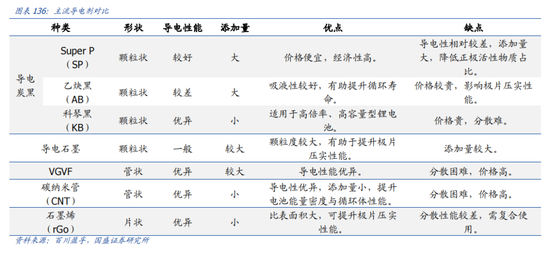
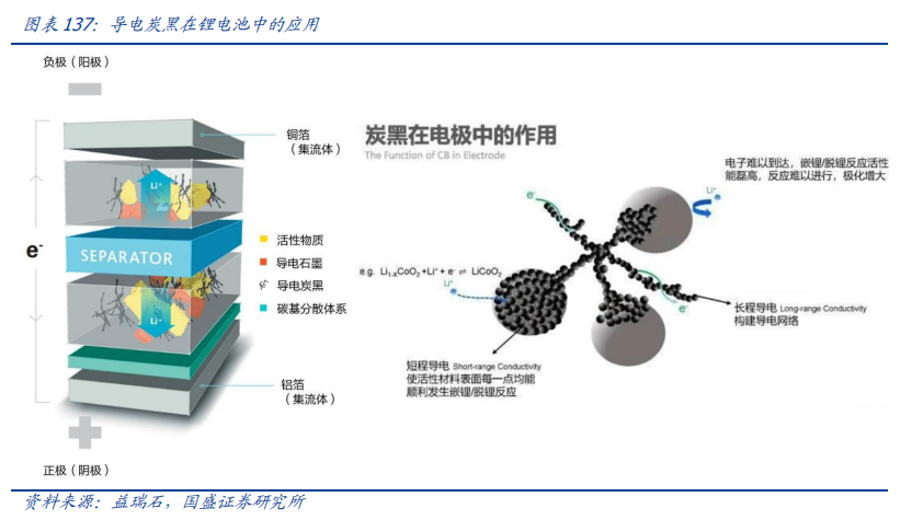 Under the trend of increasing charging performance, the amount of conductive carbon black added to fast-charging batteries and its unit value are continuously rising. The improvement in charging speed mainly depends on the charging power at the vehicle end and the battery charge and discharge rate, with the enhancement of the battery charge and discharge rate primarily reflected in battery performance. Currently, the charge and discharge rates of mainstream electric vehicles’ batteries are 1-2C, which will increase to over 4C under fast charging. To meet the increasing charging rate and the internal resistance reduction requirements brought by fast charging, the proportion of conductive agents in lithium batteries and performance requirements (unit value) are continuously increasing: ✓ Increased amount: For both positive and negative electrodes: the proportion of conductive carbon black added to the positive and negative electrodes increases compared to 2C rates; for current collectors: the carbon coating process for current collectors needs to be used in conjunction with conductive carbon black; ✓ Increased unit value: In high-rate fast-charging systems, the conductivity of traditional SP conductive carbon black cannot meet the growing performance requirements, necessitating the use of higher structural value high-performance conductive carbon black. On the pricing side: the value of high-performance conductive carbon black is significantly higher than that of traditional lithium battery-grade conductive carbon black; on the cost side: the cost of high-performance conductive carbon black compared to traditional conductive carbon black is mainly due to improvements in manufacturing processes and purification stages, thus changes in the cost side are limited; on the profit side: the combination of high value and limited cost increase significantly boosts the profitability of high-structural-value conductive carbon black compared to ordinary conductive carbon black. Breaking the overseas monopoly, focusing on the performance elasticity of leading manufacturers. Controlling indicators such as structural value and metal ion impurities in conductive carbon black is extremely challenging, and is currently monopolized by overseas companies, with mainstream manufacturers including Imerys (mainly supplying Super-P), Japan’s Lion (mainly supplying Ketjenblack), Cabot, etc., where the main supplier of lithium battery-grade conductive carbon black is Imerys. Domestic conductive carbon black started relatively late, with most players focusing on applications in cable shielding materials, coatings, conductive plastics, etc.
5
Advanced Packaging Materials
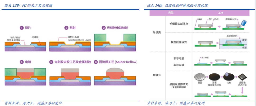
Advanced packaging is developing rapidly, and the growth potential of new packaging materials is worth looking forward to. Advanced packaging has two main development lines: one is the process of handling first and then cutting, with typical examples including FC (C4/flip chip), FI/FO-WLP (fan-in/out wafer-level packaging), TSV (through-silicon vias), and RDL (re-distribution layer); the other is stacking in a three-dimensional manner, with typical methods including 2.5D/3D packaging. Currently, the most advanced packaging methods used by OSAT manufacturers are a combination of various advanced packaging processes. For example, TSMC and Intel’s advanced packaging solutions INFO, COWOS, EMIB, etc., are integrated embodiments of multiple advanced packaging processes.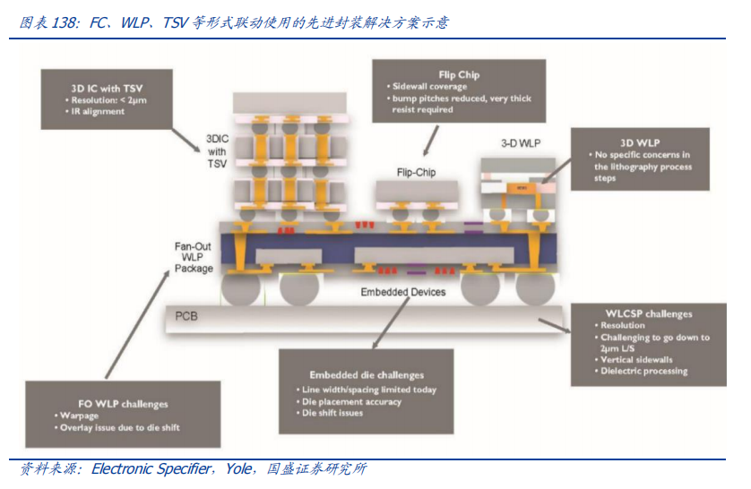 In different advanced packaging forms, various packaging materials such as DAF, TIM, underfill, temporary bonding adhesives, epoxy molding compounds, and PSPI have been applied. Combining packaging methods, we have summarized various materials used in the advanced packaging field: ✓ Underfill materials for FC flip chip: Underfill materials protect the solder bumps in FC packaging. Flip Chip is currently the most mainstream solution in advanced packaging, occupying nearly 80% of the advanced packaging market share. As the name suggests, the flip chip technology is named for flipping the bumps on the chip and installing them on substrates or other packaging bodies. Unlike WLP packaging mentioned later, although both form solder balls on the top of the wafer, the solder balls in FC packaging are smaller, with diameters of about hundreds of microns and tens of microns for WLP and FC, respectively. The significant difference in magnitude makes it difficult to ensure the reliability of solder bumps in FC packaging. The difference in thermal expansion coefficients between the chip and substrate can cause thermal stress, requiring the addition of underfill materials to disperse the stress borne by the bumps to withstand mechanical shocks.
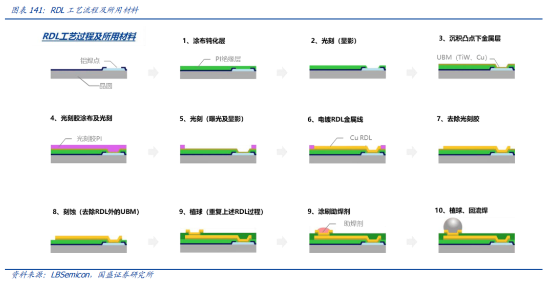
 ✓ Photo-sensitive PSPI, epoxy molding compounds EMC—WLP & RDL re-distribution: The RDL re-distribution process requires the cooperation of various materials, with PI serving as a passivation layer. The RDL technology re-layouts the I/O ports of chips by depositing metal and dielectric layers on the wafer surface and forming corresponding metal wiring patterns, re-arranging them to new areas with more relaxed space. The process first requires coating a layer of photosensitive insulating PI material over the entire wafer, followed by exposure and development. After baking, a Ti barrier layer and Cu conductive seed layer are sputtered on the formed insulating layer, and then copper is plated on the exposed Ti/Cu layer to increase the thickness of the copper layer, ensuring the conductivity of the lines. The photoresist is then stripped and etched to complete the first layer of RDL production. This process is repeated to form multiple layers of RDL lines. Finally, flux is applied to complete the ball planting. Throughout the process, multiple materials are used, including plating solutions, photoresists, stripping solutions, sputtering targets, etchants, and a photosensitive PSPI as a passivation layer.
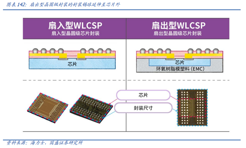
 Fan-out wafer-level packaging (FOWLP) requires the use of epoxy molding compounds as the bearing surface for RDL to prevent wafer warpage. The FOWLP process is closely integrated with RDL, where “fan-out” refers to using RDL to fan out the metal pads and solder balls from the chip to the PCB. The FOWLP can be divided into three types: face-up first chip processing, face-down first chip processing, and face-down later chip processing. In the latter type, RDL is first performed on the temporary adhesive tape surface, then the chip is interconnected with RDL in a face-down manner, followed by molding and ball planting in an injection machine to complete the cutting. The feature is that it can directly form wires and solder balls (Solder Balls) on the top of the wafer without needing a substrate, and the wafer remains intact throughout the process. The cut chips are arranged on a carrier and reconstituted into a wafer, requiring epoxy resin molding materials to fill the gaps between chips, effectively making the molding materials the bearing surface for RDL, reducing wafer warpage.
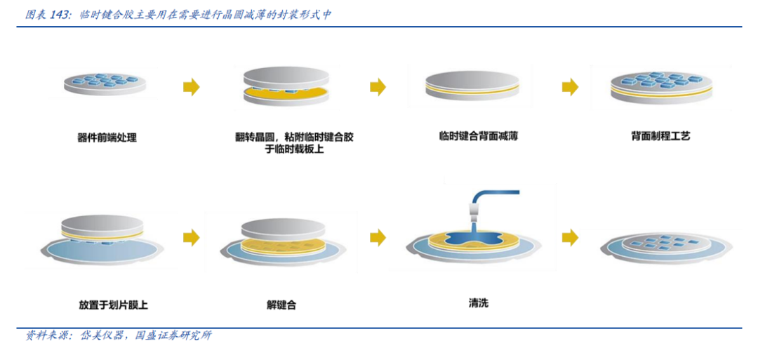
 ✓ Temporary bonding adhesive TBA—WLP & TSV silicon through-hole: In response to the trend of smaller and thinner ICs, the advent of ultra-thin wafers has driven the development of TBA materials. In wafer-level packaging, ultra-thin wafers can further reduce interconnection lengths and improve signal transmission rates. In 3D packaging, they can also reduce chip volume and enhance electrical performance. However, when silicon wafers are thinned to below 100μm, their mechanical properties significantly decrease, exhibiting characteristics such as warping and bending. In traditional packaging processes, before thinning, wafers can be attached to a dicing frame to prevent warping. However, in TSV packaging processes, since bumps form on the back of the wafer, this protection method is not applicable. Therefore, temporary bonding adhesive (TBA) serves as the intermediate layer material that bonds functional wafers to temporary carriers, ensuring that wafers do not warp after thinning. Since this bonding needs to be quickly separated after processing, temporary bonding adhesives must possess good thermal stability, mechanical stability, chemical stability, and bonding strength, while also meeting the requirement for quick removal using solvents or other means, such as thermoplastic resins that can be separated by thermal shearing, acrylic, and PI-based TBA that can be separated by laser-assisted methods, or urethane, BCB, and PI-based TBA that can be separated by chemical solvents.
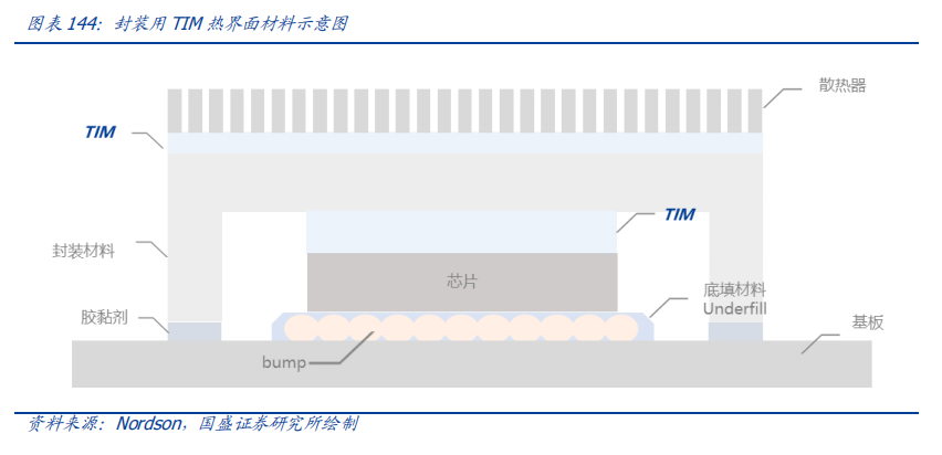
 ✓ TIM thermal interface materials: Advanced packaging systems require optimized heat dissipation paths and have higher demands for the thermal conductivity of thermal interface materials. Thermal interface materials are mainly used in the gaps between device heat sources and heat dissipation units, accelerating heat conduction from hotspots by increasing contact area. As semiconductor devices develop towards miniaturization, high integration, and high power density, their heat generation increases dramatically, but the increase in chip size is much slower. Thus, thermal failure has become the primary issue hindering the performance and lifespan of microelectronic packaged devices. High-power chips generally use a flip-chip soldering process to timely transfer heat to external heat sinks through upward heat dissipation paths. Therefore, “chip-TIM-packaging-TIM-heat sink” is the main heat dissipation path when the chip operates inside the package. Large systems (over 3 times the mask size) require higher thermal conductivity thermal interface materials (TIM) to assist in heat dissipation. According to Changjiang Electronics, liquid metal TIM has been applied in advanced packaging fields.
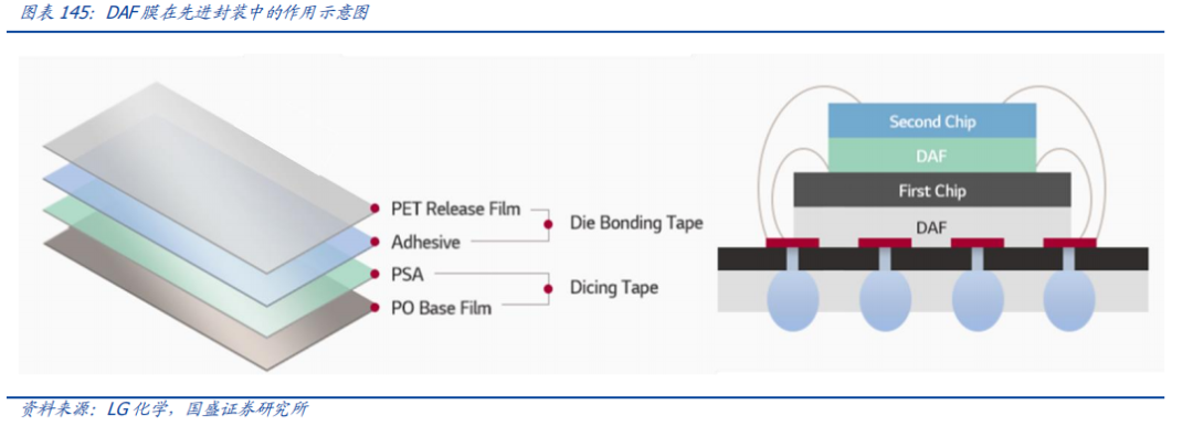
 ✓ DAF: Multi-chip stacking Chip adhesive film DAF is ultra-thin adhesive materials that achieve semiconductor packaging through layering and thinning. DAF, tightly bonded to the chip, waits for cutting processes to complete and then plays its role during the chip bonding process. As a thin film attached to the bottom of chips, DAF can be adjusted to a very small and constant thickness compared to polymer materials. Previously, it was mainly used for bonding between chips and substrates, and is now widely used in the stacking of memory chips in packaging, with some logic ICs using DAF instead of DAP to enhance packaging yield, thus forming multi-chip packaging.
 Currently, new-generation information technology, new energy, smart manufacturing, and other emerging industries are rapidly rising, combined with China’s “dual carbon” goals driving demand for new materials in the market, the position of certain key new materials in the industrial chain is becoming increasingly prominent. Energy structure reform and industrial upgrades promote the iteration of new materials and technologies, ushering in new development opportunities for the new materials industry.
(Source: Industry News)