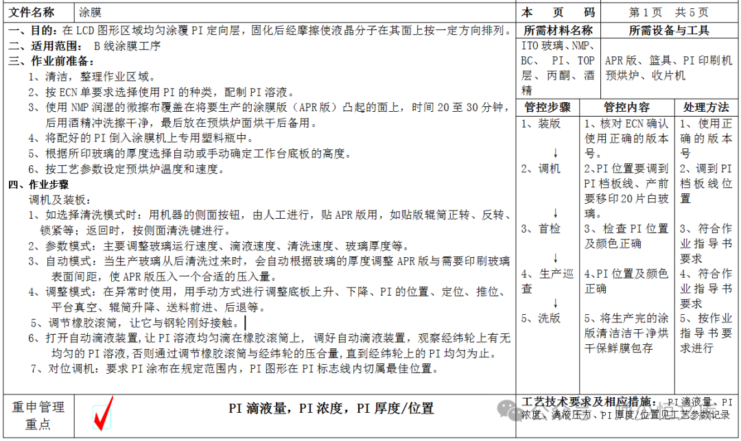
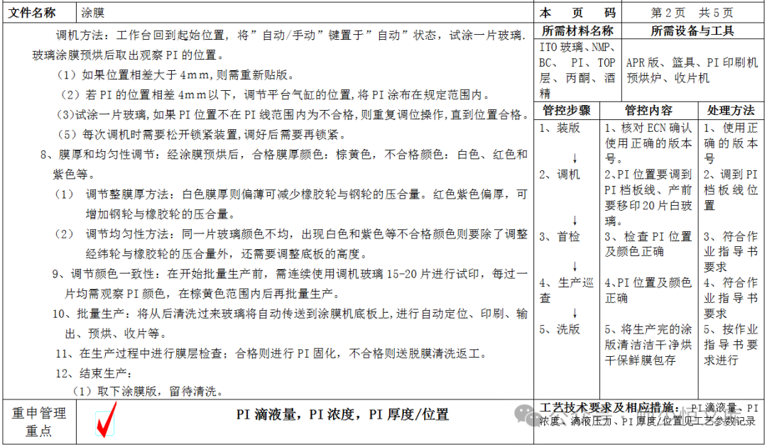
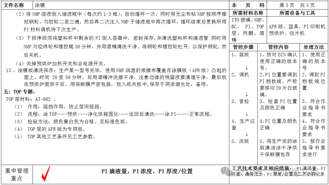
Defective products affecting the yield rate in LCD manufacturing include: ITO pinholes, scratches, insufficient corrosion, PI contamination, electrostatic breakdown, short circuits in the box, friction marks, light scratches/defects, sealing contamination, frame defects, “impact marks”, high power consumption, and display non-uniformity. Each company has its own tricks and secrets to solve these technical issues, and few have been reported.
This article mainly summarizes my personal insights on the issue of display non-uniformity. I believe that controlling the application of the insulating layer, adjusting the PI ratio, and changing the PI curing equipment are key solutions. The content is based on past experiences and is provided for reference.
1. Problem Description
1.1. Regional Brightness Differences: Certain areas of the screen are significantly brighter or darker than others;
1.2. Inconsistent Contrast: Characters or patterns have blurred or indistinct edges, or uneven contrast;
1.3. Backlight Mottling: When the backlight is on, visible light and dark stripes or spots are present.
2. Cause Analysis
Through experimental verification and data analysis, the following main causes have been identified:
2.1 Uneven distribution of liquid crystal materials: The thickness of the liquid crystal cell (Cell Gap) in STN LCDs is uneven, leading to differences in the twist angle of liquid crystal molecules; fluctuations in the infusion process parameters (such as temperature and vacuum) cause local deviations in liquid crystal layer thickness.
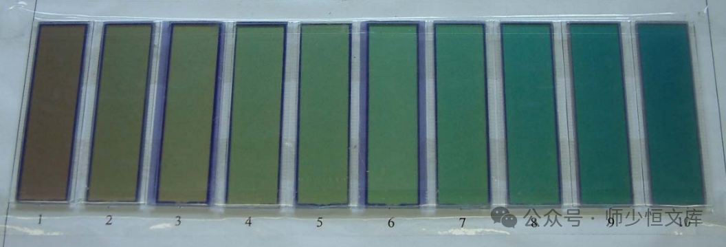
Experiments were conducted to analyze the following aspects: 1. The impact of different PIs, 2. The impact of solvent BC, 3. The impact of uneven PI film thickness, 4. The impact of PI curing temperature, 5. The impact of pressing amount, 6. The impact of the frame.
2.2 Mismatched driving voltage: The output voltage (Vop) of the driving IC does not match the threshold voltage (Vth) of the liquid crystal material; insufficient precision of the voltage divider resistors leads to voltage deviations between the common electrode (COM) and segment electrode (SEG) signals.
2.3 Design defects in the backlight module: The distribution of the dot density in the light guide plate (LGP) is unreasonable, causing uneven backlight brightness; the spacing of the LED light sources is too large or the brightness consistency is poor.
2.4 Insufficient process control: Bubbles or uneven pressure exist during the attachment of the polarizer; unstable curing conditions (temperature, time) of the sealing adhesive lead to abnormal stress distribution in the liquid crystal box.
3. Improvement Measures
3.1 Optimize the liquid crystal box process, adjust Cell Gap precision: Use high-precision spacer materials to control the liquid crystal box thickness tolerance within ±0.2μm; improve the infusion process: add dynamic pressure monitoring during the vacuum infusion phase to ensure uniform filling of the liquid crystal material.
3.2 Improve the driving circuit, voltage compensation design: Add a voltage feedback module in the driving circuit to adjust Vop voltage in real-time, matching the liquid crystal response characteristics of different areas; enhance the precision of voltage divider resistors: improve the precision from ±5% to ±1%, and add a temperature compensation circuit.
3.3 Optimize the backlight module, redesign the dot distribution of the light guide plate: Use optical simulation software (such as LightTools) to optimize dot distribution and balance brightness differences between edges and centers; select LED light sources: use LEDs with brightness sorted by bin to ensure that the brightness consistency of a single batch of light sources is ≤5%.
3.4 Standardize process parameters, polarizer attachment process: Introduce automatic alignment equipment, control the attachment pressure at 0.3±0.05MPa to eliminate bubbles; control curing conditions: adjust the curing temperature of the sealing adhesive from 25℃±5℃ to 25℃±1℃, and extend the time to 30 minutes.
4. Verification Results
After implementing the improvement measures, the verification results are as follows: This improvement significantly reduced the display non-uniformity issue by optimizing the liquid crystal box process, driving circuit, and backlight design. In the future, we will: incorporate the improvement measures into the standard operating procedures (SOP) for mass production; regularly monitor key process parameters (such as Cell Gap, driving voltage); and develop automated optical inspection (AOI) equipment to achieve 100% inspection.