-
Video Stream
-
Pixel Clock
-
Display Parameter Analysis
-
D-PHY Principles
-
Link Basics
-
Operating Modes
-
I/O Signals
-
DDR (Dual Data Rate) Transmission Method
Video Stream
All modern computer displays are raster displays, meaning that the images displayed are created by writing pixel by pixel from left to right and from the top of the display to the bottom, line by line. The displayed image or frame consists of a rectangular array of pixels. A video stream is composed of a series of frames displayed at fixed time intervals. This time interval can be described in Frames Per Second (FPS) or Hz. The roots of this process can be traced back to old cathode ray tube displays.
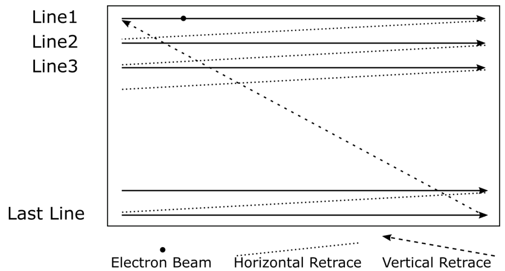
The operation of LCD and OLED displays is derived from traditional CRT display technology, as shown above. They illuminate images frame by frame by continuously scanning the back of the screen with an electron beam. The specific process is as follows:
The display of each frame of the image is accomplished by filling pixels line by line from left to right and from top to bottom until the entire screen is filled. The electron beam first scans a line of the image from left to right and lights it up. After the line scan is complete, the electron beam turns off and returns horizontally to the left side of the screen to prepare for the next line scan. The electron beam then scans the entire screen line by line from top to bottom, ultimately completing the display of one frame of the image.
After completing the display of one frame of the image, the display system continuously shows multiple frames to generate a continuous and complete visual effect.
This line-by-line scanning mechanism determines that the display system needs to introduce some synchronization signals and timing parameters to ensure the stable operation of the electron beam, thereby achieving good display effects.
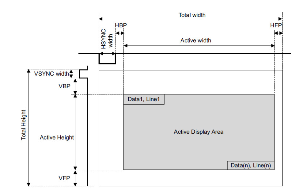
The action of returning to the left side and back to the first line mentioned here cannot be completed instantaneously and requires a certain amount of time. Therefore, we introduce the following parameters to ensure a stable beam for display:
- HFP (Horizontal Front Porch) – The front porch of the horizontal sync signal, representing the number of pixels not displayed after the effective pixel data ends, which is also the time interval required for the beam to turn off and return.
- H-SYNC (Horizontal Sync) – Sent before the start of each line, the time required for the beam to traverse the screen horizontally.
- HBP (Horizontal Back Porch) – The back porch of the horizontal sync signal, representing the invalid lines after the horizontal sync signal, ensuring that the beam is stable when lighting up the next line. After the HBP signal, the first valid display pixel begins to be sent.
- HACTIVE – Horizontal active pixels.
The switching between frames also requires a certain amount of time, and we introduce the following parameters to ensure a stable beam for display:
- VFP (Vertical Front Porch) – The front porch of the vertical sync signal, representing the invalid data lines from the end of the current frame data output to the start of the next frame vertical sync period, which is also the time required for the beam to return. After the VFP signal, the next frame begins scanning.
- V-SYNC (Vertical Sync) – Sent before the display of each frame, ensuring the time interval required for the beam to return vertically from the bottom of the screen to the top.
- VBP (Vertical Back Porch) – The back porch of the vertical sync signal, representing the invalid lines after the vertical sync signal. Similar to the previous HBP function, it is the time required to ensure beam stability. After the VBP signal, the first valid pixel line begins to be sent.
- VACTIVE – Vertical active pixels.
Pixel Clock
The clock must sequentially preserve pixel data and synchronization signals. This clock is called the pixel clock. One pixel is transmitted per clock cycle. It is the main clock for most image display transmission systems. In the case of image sensors, the pixel clock time period sets the ADC conversion time interval for each pixel. It is the root clock for HSYNC and VSYNC signals. The HSYNC signal indicates the start of each line, while the VSYNC signal indicates the start of each new frame.
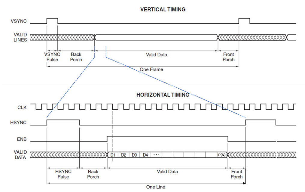
The ENB signal is used to indicate active pixel data transmission. Without this signal, various pixel pipelines may misinterpret blanking data as pixel data with a value of 0.
Display Parameter Analysis
Display parameters usually need to be included in the driver or DTB corresponding to the screen used by the customer. The following is an example using the RM67191 MIPI-DSI screen:
#gpu/drm/panel/panel-raydium-rm67191.c
static const struct drm_display_mode default_mode = {
        .clock = 121000,
        .hdisplay = 1080,
        .hsync_start = 1080 + 20,
        .hsync_end = 1080 + 20 + 2,
        .htotal = 1080 + 20 + 2 + 34,
        .vdisplay = 1920,
        .vsync_start = 1920 + 10,
        .vsync_end = 1920 + 10 + 2,
        .vtotal = 1920 + 10 + 2 + 4,
        .width_mm = 68,
        .height_mm = 121,
        .flags = DRM_MODE_FLAG_NHSYNC |
                 DRM_MODE_FLAG_NVSYNC,
};
The screen parameters are sometimes provided separately as individual parameters. In the new version of the BSP, they need to be provided through the above hsynchronization_start, hsynchronization_end, and other parameters. The specific meanings and provision requirements of each parameter can be referenced in the documentation of the DRM-related driver:
/**
 * linux-imx/include/uapi/drm/drm_mode.h
 * struct drm_mode_modeinfo - Display mode information
 * @hdisplay: horizontal display size
 * @hsync_start: horizontal sync start
 * @hsync_end: horizontal sync end
 * @htotal: horizontal total size
 * @hskew: horizontal skew
 * @vdisplay: vertical display size
 * @vsync_start: vertical sync start
 * @vsync_end: vertical sync end
 */
From the above RM67191 and DRM driver, we obtain the screen-related parameters for RM67191 as follows:
HFP = 20
H-SYNC = 2
HBP = 34
HACTIVE = 1080
VFP = 10
V-SYNC = 2
VBP = 4
VACTIVE = 1920
When integrating the display screen into the system, the following steps need to be followed:
-
Obtain the various timing parameters involved from the screen’s datasheet and technical specifications, including horizontal and vertical blanking intervals, the number of active pixels, etc. These parameters are necessary for configuring the screen driver.
-
In the display device’s driver, configure and initialize the relevant registers or variables according to the timing parameters obtained from the datasheet. For example, set the values of HFP, H-SYNC, HBP, HACTIVE, and other horizontal parameters.
-
At the same time, in the device tree (DTB), these timing parameters also need to be configured and declared so that the operating system can correctly recognize and drive the display device.
After completing the configuration of the above driver and device tree, the system can correctly initialize and light up the connected display screen.
In summary, correctly obtaining the technical parameters of the display screen and accurately configuring them in the driver and device tree is key to successfully integrating the display device. Only in this way can the system stably output the expected image effects.
D-PHY Principles
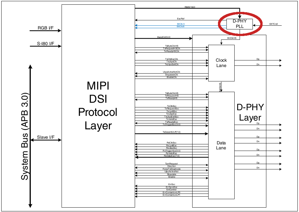
As can be seen from the figure, the display process of the MIPI-DSI interface can be divided into two parts:
- D-PHY: This is the source-synchronous physical layer used by the CSI-2 and DSI protocols, responsible for handling physical and electrical communication.
- Display Serial Interface (DSI): This is the interface between the processor and peripherals, established based on existing specifications from the MIPI Alliance.
This article will first introduce the working principles of D-PHY.
Link Basics
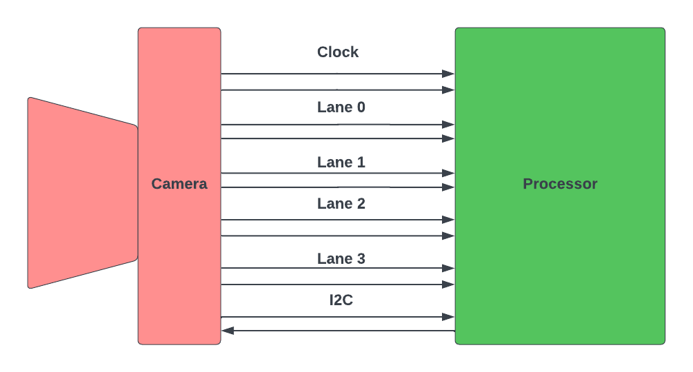
The MIPI specification uses a consistent set of terms when discussing the components required for assembling systems based on CSI-2 or DSI.
- Line: The interconnection, wire, or lead between a single pin of the main processor and a pin of a peripheral device.
- Lane: Two lines are needed to support differential signals. D-PHY uses differential pairs for high-speed data and clock transmission. This differential pair is referred to as lane interconnect, but is mostly abbreviated as lane in technical documentation.
- Link: The connection between two devices that includes one clock lane and at least one data lane. A link must include at least two PHYs and two channel interconnects.
Operating Modes
There are four operating modes:
- Control Mode
- High-Speed Mode
- Escape Mode
- Ultra-Low Power State (ULPS) Mode.
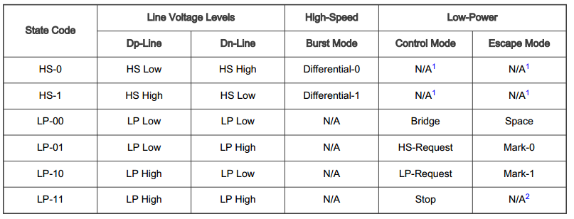
The data lane supports all four modes, but the clock lane only supports control mode, high-speed mode, and ultra-low power state mode. During normal operation, the data lane is in control mode or high-speed mode. The high-speed data transmission mode is adopted during data bursts, starting from the stop state of control mode (LP-11) and ending in the stop state of control mode (LP-11). The lane is only in high-speed mode during data bursts. The following table describes the six physical states that the clock and data lanes can enter.
During normal operation, the data lane continuously switches between low-power control mode and high-speed data transmission mode.
I/O Signals
D-PHY IO pins have two different electrical operating modes: single-ended mode and differential mode.
- Single-ended mode is called low-power (LP) mode, used for escape mode and control mode, for system configuration/control between the main processor and peripheral devices. In LP mode, the IO circuits use traditional CMOS output buffers (with slope control), switching between ground and VDD_IO. In LP mode, the two IO circuits that make up the lane can switch independently. They provide four different lane states: LP-00, LP-01, LP-10, and LP-11.
- Differential mode is called high-speed (HS) mode, used only for data transmission. Differential mode has only two states: HS-0 and HS-1. In HS mode, the two IO circuits that make up the lane always output opposite polarities and cannot both be high or low at the same time. The following diagram illustrates the difference in signal levels between HS and LP modes.
During normal operation, the data lane continuously switches between low-power control mode and high-speed data transmission mode.
DDR (Dual Data Rate) Transmission Method
- In a single data rate (SDR) synchronous data bus architecture (e.g., SDRAM), data is sampled on either the rising or falling edge, but not on both. This means that the data rate equals the clock speed. Various low-power modes use a single data rate clock structure.
- The DDR (dual data rate) bus architecture can transmit data on both clock edges, not just on a single edge. Data transmission in HS mode uses the DDR transmission scheme. This means that for a given clock frequency (Fr), the data rate for each channel is 2 × Fr.
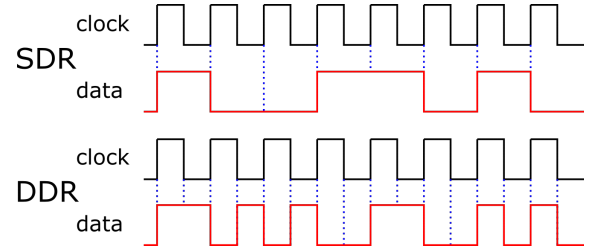
In the high-speed data transmission mode (High-Speed, HS) architecture, the data lane generally adopts dual data rate (DDR) transmission technology. The core of this technology is that data sampling operations occur not only on the rising edge of the clock signal (CLK Lane) but also synchronously on the falling edge, achieving two samples per clock cycle, effectively doubling the data transmission efficiency. Specifically, whenever the state of the CLK Lane changes from low to high (rising edge) or from high to low (falling edge), the data on the Data Lane is captured and transmitted.
Therefore, if the nominal frequency of the CLK signal is F Hz, then in DDR mode, the actual data transmission rate for each data lane reaches 2F bps (bits per second), effectively doubling the frequency. This characteristic is particularly important when evaluating and calculating the clock frequency of the Mobile Industry Processor Interface (MIPI), where DRPL (or Bit Clock) directly reflects the data rate, and its value divided by 2 gives the equivalent frequency of the MIPI Clock, reflecting the conversion relationship between the internal processing clock signal and the data rate.
In summary, DDR transmission technology achieves a doubling of the data transmission rate by sampling data on both the rising and falling edges of each clock cycle. This mechanism is widely used in high-speed data transmission systems, especially in the design and implementation of standards such as MIPI.
end
One Linux
Follow, reply with 【1024】 to receive a wealth of Linux materials
Collection of Wonderful Articles
Article Recommendations
☞【Collection】ARM☞【Collection】Fan Q&A☞【Collection】All Originals☞【Collection】LinuxIntroduction☞【Collection】Computer Networks☞【Collection】Linux Drivers☞【Essentials】Embedded Driver Engineer Learning Path☞【Essentials】All Knowledge Points of Linux Embedded – Mind Map