Source: An Introduction to SPI Communications Protocol
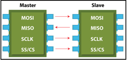
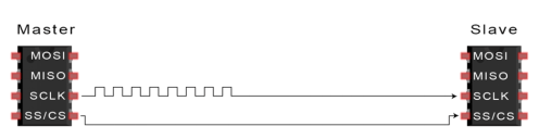
SPI is a full-duplex, synchronous, master-slave interface, involving two main roles: master device and slave device. The SPI interface can be 3-wire or 4-wire, with a focus here on the commonly used 4-wire SPI interface. The 4-wire SPI interface has four signals: clock signal (SCLK), slave select signal (SS/CS), master out slave in signal (MOSI), and master in slave out signal (MISO), as shown below:
Source: SPI Protocol – Serial Peripheral Interface – javatpoint
Among them,
-
SCLK (Serial Clock): The clock signal line provided by the master device for synchronizing data transmission.
-
MOSI (Master Out, Slave In): The line for the master device to send data to the slave device.
-
MISO (Master In, Slave Out): The line for the slave device to send data to the master device.
-
SS (Slave Select): The signal line controlled by the master device to select the slave device to communicate with.
1) Single Master Single Slave Mode
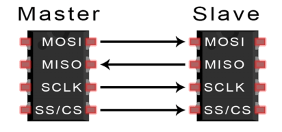
In single master single slave mode, the master’s SCLK, MOSI, and MISO are connected to the corresponding pins of the slave device. There is only one set of SCLK, MOSI, and MISO lines connected between the master and slave devices, as shown below:
Source: Basics of the SPI Communication Protocol (circuitbasics.com)
The basic principle is:
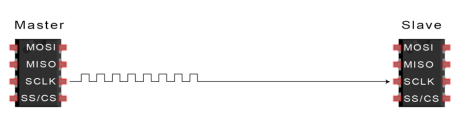
First is clock synchronization, where the master device generates SCLK to control the timing of data transmission. The clock signal is provided by the master device and is synchronized between the master and slave devices.
Source: Basics of the SPI Communication Protocol
Then comes the slave select signal, where the master device switches the SS/CS pin to a low voltage state to activate the slave device.
Source: Basics of the SPI Communication Protocol
Finally, during the data transmission process, the master device sends data to the slave device through the MOSI line. After the slave device receives the data, it transmits it back to the master device through the MISO line. Data transmission between the master and slave devices occurs simultaneously.
Source: Introduction to SPI Interface | Analog Devices
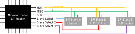
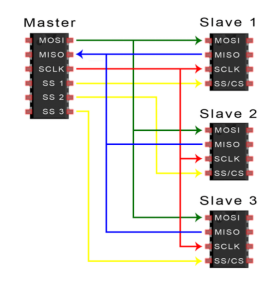
2) Single Master Multiple Slaves Mode
In single master multiple slaves mode, the master’s SCLK and MOSI are connected to the corresponding pins of each slave device, and the slave devices’ MISO are connected to the master’s MISO pin. Each slave device has an independent SS pin connected to the master device, which the master uses to select the slave device it wants to communicate with.
Source: Basics of the SPI Communication Protocol
The basic principle is almost the same as in single master single slave mode, with the only difference being that when a slave device’s SS is low, that slave device communicates with the master device, while the SS of other slave devices remains high.
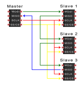
3) Daisy Chain Mode
In daisy chain mode, the master’s MOSI and SCLK are connected to the first slave device’s MOSI and SCLK. The first slave device’s MISO is connected to the second slave device’s MOSI, and so on, until the last slave device’s MISO.
Source: Basics of the SPI Communication Protocol
The working principle is:
First, the master device provides SCLK, controlling the timing of data transmission. The clock signal is generated by the master device and is passed throughout the daisy chain, with slave devices transmitting and receiving data based on the edges of the clock signal.
Then, the master device sends data to the first slave device via the MOSI line. The first slave device receives the data and transmits it to the second slave device through the MISO line, thus cascading the data from one slave device to the next until it reaches the last slave device.
Each slave device needs to have an independent SS; the master device selects which slave device to communicate with by controlling the corresponding SS. Only the selected slave device will respond to the master’s data transmission.
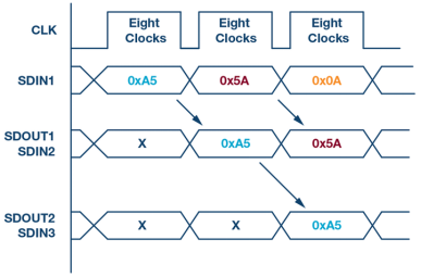
In daisy chain mode, the number of clock cycles required for data to propagate from one slave device to the next is proportional to the position of the slave device in the chain. In an 8-bit system, the data on the third slave device requires 24 clock pulses, while in conventional SPI mode, only 8 clock pulses are needed. The following diagram shows the clock cycles and data propagated through the daisy chain.
Source: Introduction to SPI Interface | Analog Devices
Source: What Could Go Wrong: SPI | Hackaday
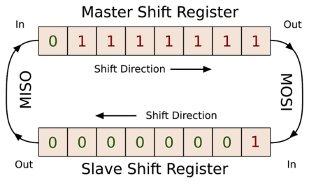
4.1 Sampling and Shifting
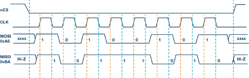
As mentioned above, during SPI communication, the master device must send the SCLK signal and select the slave device by enabling the SS signal (low level). The master and slave devices can then send data simultaneously through the MOSI and MISO lines. During SPI communication, sending data (shifting out to the MOSI/SDO bus) and receiving data (sampling or reading data on the MISO/SDI bus) occur simultaneously.
> Sample
Sampling refers to the operation where the master or slave device reads the data bits at the rising or falling edge of the clock. The purpose of sampling is to capture the correct data bits at the right time to ensure accurate data transmission.
> Shift
Shifting refers to the process of moving data bits from the sender to the receiver to achieve data transmission. Shifting is one of the key steps in SPI communication, ensuring bit-by-bit transmission and synchronization of data.
4.2 Clock Polarity and Clock Phase
When to perform sampling and shifting operations can be achieved by setting the clock polarity and clock phase.
> Clock Polarity (CPOL)
The CPOL bit sets the polarity of the clock signal during idle state.
CPOL = 1: indicates high level during idle;
CPOL = 0: indicates low level during idle.
The idle state refers to when CS is high at the start of transmission and transitions to low, and when transmission ends with CS low transitioning to high, as shown below:
> Clock Phase (CPHA)
The CPHA bit selects the clock phase. Depending on the state of the CPHA bit, either the rising or falling edge of the clock is used to sample and/or shift data.
CPHA = 0: indicates sampling starts from the first transition edge;
CPHA = 1: indicates sampling starts from the second transition edge.
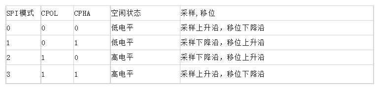
The master device must select the clock polarity and clock phase according to the requirements of the slave device. Based on the selection of CPOL and CPHA bits, four SPI modes are available, as shown below:
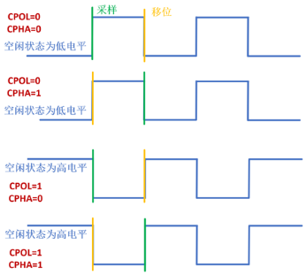
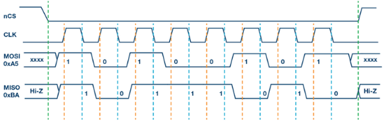
Corresponding to the data bits, taking CPOL = 0, CPHA = 0 as an example, the green dashed line represents SS enable, the orange dashed line represents sampling, and the blue dashed line represents shifting, as shown below:
Source: Introduction to SPI Interface | Analog Devices
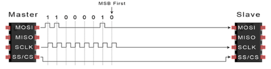
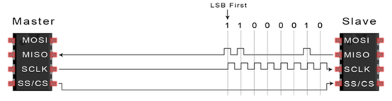
4.3 Bit Order of Transmission
Whether to send the high bit (MSB) first or the low bit (LSB) first. As shown in the following diagram, if MSB first is adopted, then the data sent by MOSI is 01000011, i.e., 0x43.
Source: Basics of the SPI Communication Protocol
If LSB first is adopted, then the MISO will send the following after receiving 0x43:
Source: Basics of the SPI Communication Protocol
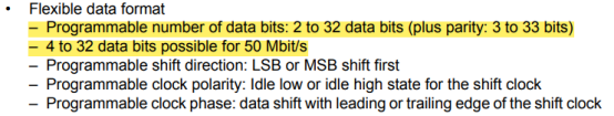
4.4 Data Length
Note that the above diagrams demonstrate the transmission of 8-bit data, while SPI can transmit different bit lengths depending on the device’s capabilities; for instance, the Aurix TC2xx series supports up to 32-bit data transmission.
In summary, SPI data transmission depends on specific configurations, such as which mode to select, when to sample, how many bits of data, and whether to use MSB or LSB first. Additionally, there are more factors to consider when implementing this functionality.
This article has introduced the basic content of SPI in a relatively easy-to-understand way, specifically how to achieve data transmission between master and slave devices through four signal lines (SCLK, SS, MISO, MOSI) in conjunction with shift registers; regarding how to configure data transmission, parameters such as clock polarity and clock phase need to be set. For those who wish to delve deeper into this topic, please refer to the following content:
Author: 糊涂振, Source: Automotive Electronics and Software