AI is empowering mobile phones to become personal intelligent terminals, driving growth in the mobile phone market. In the previous article, we detailed how NPUs provide energy efficiency far exceeding that of CPUs/GPUs through three major designs: fixed computation flow, tightly coupled memory, and mixed low-precision inference, making it a core upgrade direction for mobile hardware.
The upgrade of NPUs comes not only from terminal SoC manufacturers but also from the underlying instruction sets and IP licensing. In the current stagnation of mobile phone shipments, IP cores, with their highly profitable model of one-time licensing and unlimited reuse, have become the most certain beneficiaries in the existing market—ARM’s IP cores can bring continuous royalty income with marginal costs approaching zero. The now-popular AI chip company Cambricon also started with the IP licensing model.This article, as the second part of the evolution of SoCs, will focus on the business model of IP licensing. By dissecting the business strategies of industry leader ARM, we will analyze how the IP licensing track generates profits and explore companies with IP core design capabilities and investment opportunities in the context of NPU upgrades.
Table of Contents
1. Classification of IP Cores
2. ARM’s Business Model
3. Industry Landscape
1. Classification of IP Cores
Despite the empowerment of AI, the smartphone industry has ultimately entered a mature stage after more than a decade of development, with a clear market ceiling, exhibiting typical characteristics of a saturated market: major brands are fiercely competing in product, performance, and sales, yet it is difficult to significantly boost overall market growth.
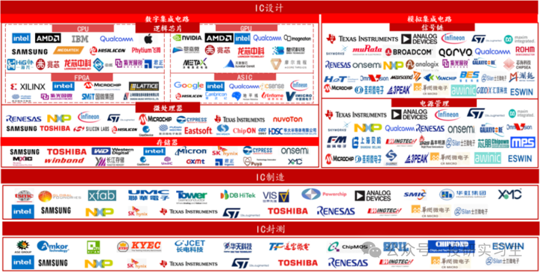
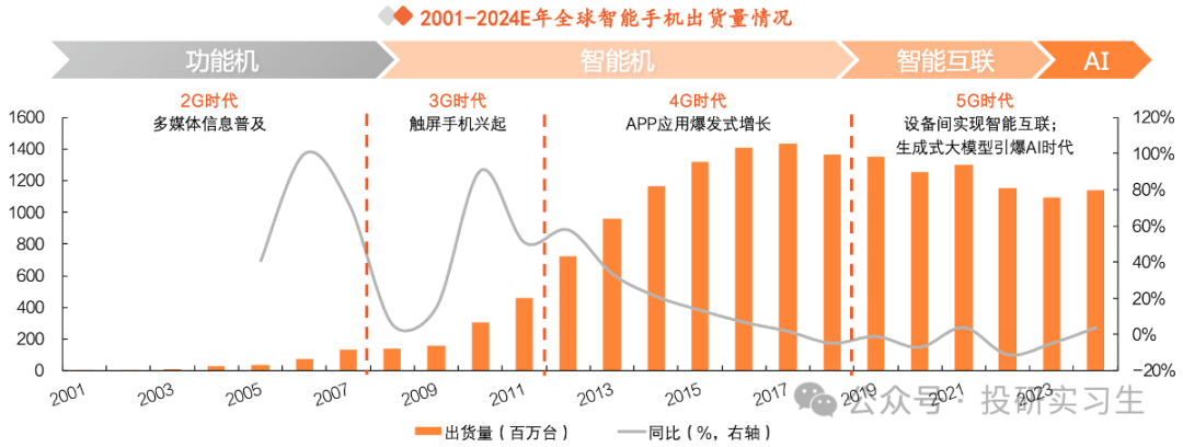 As NPUs become the core direction for the next generation of AI mobile hardware upgrades and a key support for differentiated products, combined with the highly profitable business model of IP core licensing, the NPU design track has a good positioning advantage and is expected to become the biggest beneficiary in the industry chain under the narrative of AI mobile.First, let’s take a look at what IP cores are and their role in the semiconductor industry chain.The semiconductor industry chain is divided into three main stages: upstream design, midstream manufacturing/testing, and downstream applications. IP cores belong to the upstream design stage and are pre-designed and verified functional modules that provide core design components for chip design manufacturers, positioned at the very top of the industry chain.
 IP cores can be classified by delivery method and product type. By delivery method, they can be divided into soft cores, firm cores, and hard cores; by product type, they can be divided into processor IP, interface IP, other physical IP, and other digital IP.
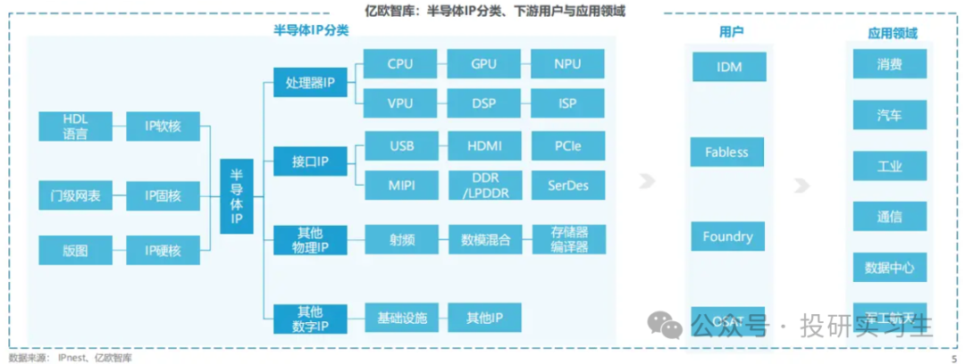 From the definition, soft cores refer to code written in hardware description language, hard cores refer to physical layouts made in conjunction with manufacturing processes, which is the physical implementation of the code. Firm cores are in between soft and hard cores, referring to gate-level netlists with layout planning. Let’s start from the chip design process to see what soft cores, hard cores, and firm cores specifically are.The chip design process is divided into five stages: first is functional definition and implementation, followed by verification, logic synthesis, physical implementation, and tape-out, where the most important stages are functional definition, logic synthesis, and physical implementation.
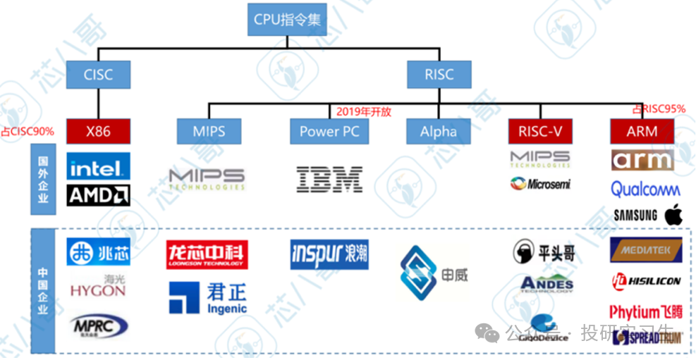
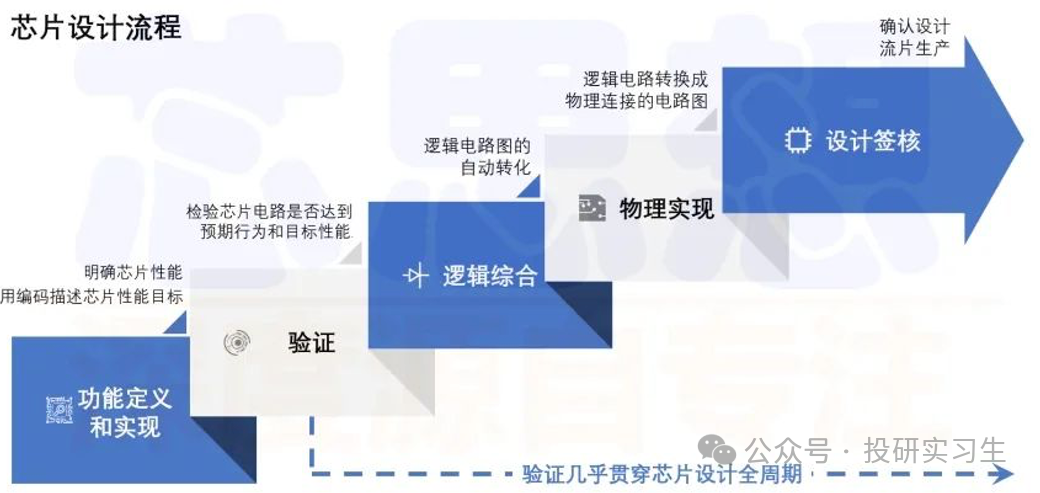 Functional definition, as the initial stage, requires chip design companies to analyze requirements by clarifying the market positioning, performance and power consumption targets, cost budget, and other directions. For example, if we want to create an AI mobile SoC, it should support running large models on the edge, achieving a computing power of 50 TOPS, with power consumption below 5W, using a 3nm process, and keeping BOM costs controllable.After clarifying the requirements, the corresponding instruction set architecture must be selected, which is the language that enables communication between the chip’s hardware and software. Instruction sets are divided into Complex Instruction Set Computing (CISC) and Reduced Instruction Set Computing (RISC). CISC is mainly the x86 architecture dominated by AMD and Intel, while RISC includes ARM’s architecture and the open-source RISC-V architecture.The x86 architecture is characterized by complex instructions, where a single instruction can perform many operations, thus having strong performance, but it also has issues of high power consumption and complex design. The x86 architecture is the dominant force in the PC and server markets, especially before the explosion of the mobile market, having built a large ecosystem on PCs and servers through its deep integration with Windows.
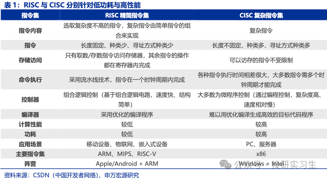 In contrast to x86, the ARM architecture, which belongs to RISC, is characterized by simplified instructions, high execution efficiency, and low power consumption. Mobile devices have much higher power consumption requirements than PCs and servers, which is why ARM has dominated the mobile market during the smartphone era. For instance, Apple’s self-developed mobile and computer chips and NVIDIA’s CPUs are all based on the ARM architecture.
 After selecting the appropriate instruction set architecture, the logic synthesis stage begins, also known as front-end design, which mainly addresses the logical functionality of the chip. Front-end design involves writing code, also known as RTL coding, using hardware description languages (mainly Verilog) to describe various logical functions.
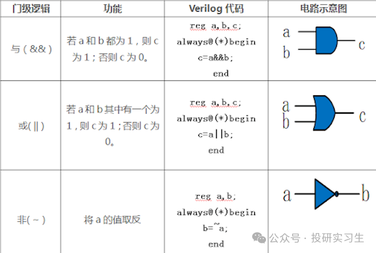 Soft cores (Soft IP) are the RTL code that chip design companies can directly deliver to downstream companies, which then integrate it with other modules’ RTL code. Since soft cores are only design at the code level and do not include physical design, the actual performance, area, and other attributes of the chip are unknown.With the RTL code, EDA design tools can automatically convert it into a logic circuit, also known as a gate-level circuit netlist, which is composed of various logic gates. Chip manufacturing factories provide standard cell libraries to translate RTL code into gate-level circuit nets.
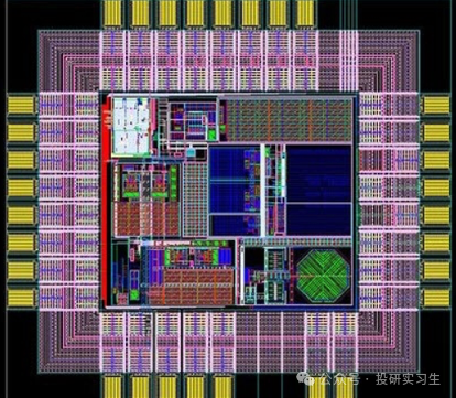
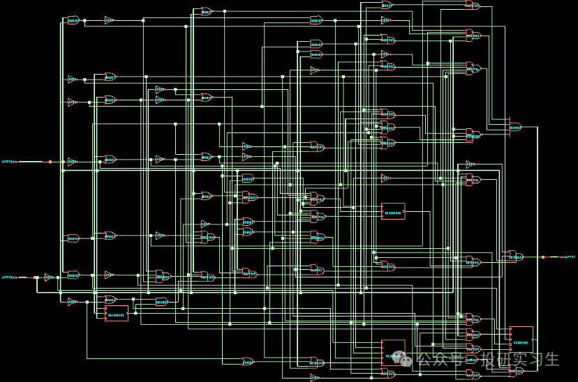 The delivery method of firm cores (Firm IP) is the delivery of gate-level netlists, which are more predictable in performance and area than soft cores.The gate-level circuit netlist must undergo static timing analysis (STA) and formal verification tests, and after confirming that it meets the requirements, it is formally input to the back-end design, which is the physical implementation of the chip.Physical layout design must consider various complex physical factors such as transistor size, shape, and wiring length when determining the specific positions of each module on the chip, mainly including cell layout, clock tree synthesis, and routing design.Once the physical layout is designed, as shown in the figure below, hard cores (Hard IP) are the designed physical layouts delivered in GDSII file format. At this point, the chip’s size, shape, performance, and other attributes are completely fixed and cannot be modified, relying on specific manufacturing processes.
 Finally, after further physical verification, the physical layout can be sent to the wafer manufacturing plant for tape-out, or trial production. Only designs that successfully pass tape-out can proceed to final mass production.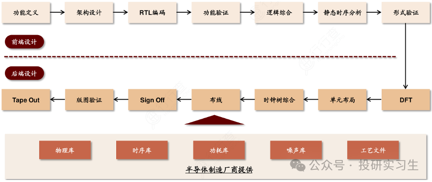
2. ARM’s Business Model
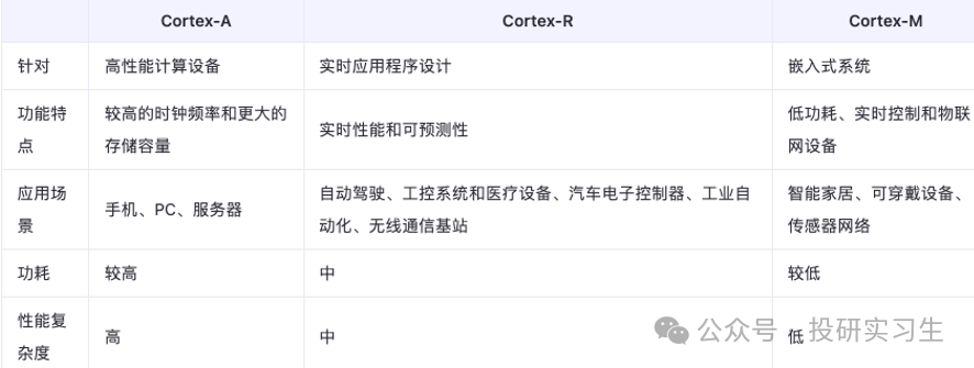
How does a company that designs IP cores but does not participate in chip design make money? Next, we will understand the IP licensing business model by dissecting the business strategies of the leading company in the IP core track, ARM.(1) History of ARMFirst, let’s look at the history of ARM. ARM was established in 1990, headquartered in the UK, and originated from Acorn Computers, founded in 1978. In 1985, Acorn’s engineering team developed the Acorn RISC Machine (also known as ARM 1), which used Reduced Instruction Set Computing (RISC) and was manufactured by VLSI Technology in the UK (now NXP Semiconductors).The first-generation ARM 1 coincided with the peak of Intel, whose 80386 processor launched in the same year outperformed ARM 1. Soon, Acorn, which was forced into a financial crisis by Intel in 1980, was acquired by Olivetti, and subsequently launched ARM 2 and ARM 3 in 1986 and 1989, respectively.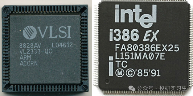 In 1990, Acorn, along with VLSI and Apple, established the new ARM company, officially named Advanced RISC Machines Ltd, with its main business focused on developing and designing chips based on the ARM architecture and corresponding IP licensing.Learning from the early lessons of Acorn being beaten by Intel, ARM took a different path from the beginning, no longer designing and manufacturing chips itself, but uniquely creating a business model for licensing processor architecture design solutions.In this model, ARM operates lightly, avoiding competition with terminal chip design manufacturers, naturally not bearing the enormous costs and risks of chip manufacturing and sales, while also being able to focus better on processor architecture design.Before 2004, ARM’s product line underwent iterations of ARM 6, ARM 7, ARM 9, etc., and its architecture evolved from ARM V3 to V. In 2004, to enrich downstream application scenarios, ARM made significant reforms to its product line, launching the Cortex series, dividing CPUs into three categories: Cortex-A (application processors), Cortex-R (real-time processors), and Cortex-M (microcontrollers).The Cortex-A series targets high-performance application processors, supporting complex operating systems, suitable for smartphones, tablets, and high-performance computing devices. The Cortex-R series targets real-time control processors, emphasizing low latency and reliability, suitable for automotive electronics, industrial control, and communication devices. The Cortex-M series targets low-power microcontrollers, suitable for IoT and embedded devices.
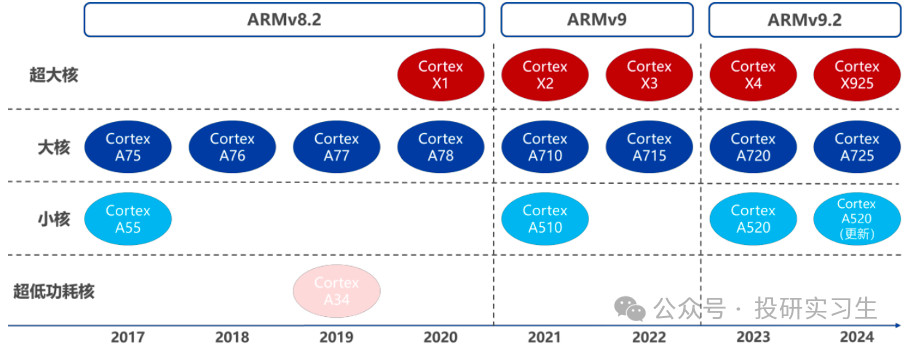
 In 2011, ARM released its first architecture supporting 64-bit instruction sets, ARMv8, marking the entry of ARM architecture into the high-performance and 64-bit computing stage. The most representative products of ARMv8 are the Cortex-X series high-performance super cores launched in 2020, such as the flagship processors Snapdragon 888, MediaTek 9000, and Apple M1, which all use Cortex-X1 and Cortex-X2.
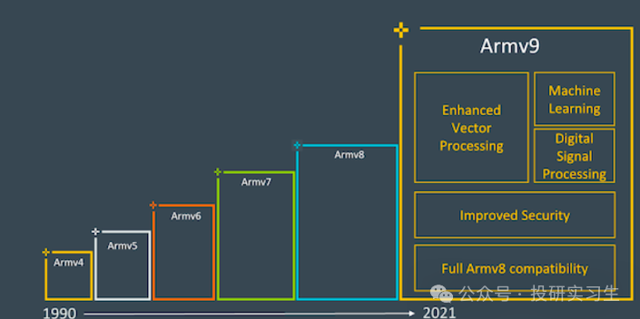
 In 2018, ARM introduced the Neoverse series CPU IP cores based on the Cortex series, specifically designed for infrastructure fields such as servers and data centers. Its Neoverse N1 and N2 products are used by cloud providers including Amazon AWS Graviton and Alibaba’s T-Head, while Neoverse CSS is used by NVIDIA’s Grace CPU.In 2021, ARM released the next-generation architecture ARMv9, marking the entry of ARM architecture into the AI and heterogeneous computing stage. ARMv9 enhances processor performance while improving security, vector computing, machine learning, and digital signal processing capabilities.
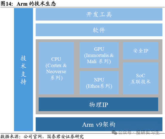
 At the same time, ARM also launched the Mali series and Immortalis series GPU product lines, as well as the Ethos series NPU product line, specifically designed for AI computing.
 With its low power characteristics and flexible licensing strategy, the ARM architecture rapidly rose during the mobile internet era. Today, over 99% of smartphone processors globally are based on the ARM architecture, and its ecosystem is expanding into PCs, servers, and other fields.
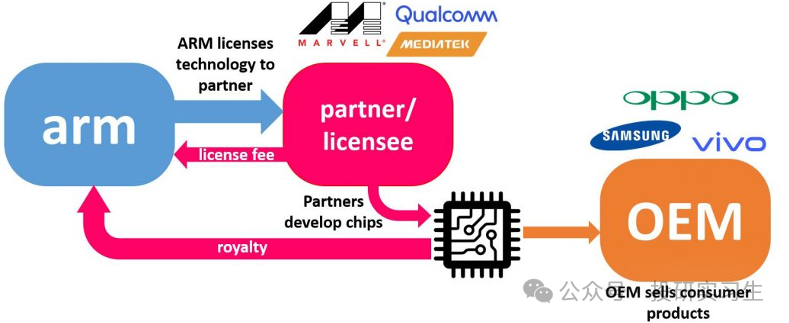
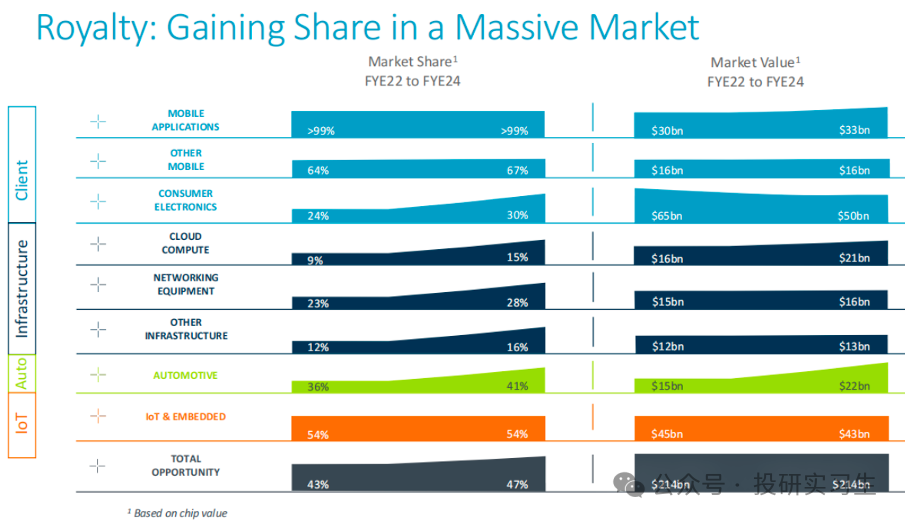 The rise of ARM is in stark contrast to Intel, which has continuously struggled in the mobile sector. As the saying goes, “Thirty years in the east, thirty years in the west,” the Intel that once dominated ARM is now being countered by ARM.In 1998, ARM was listed on the London Stock Exchange, and in 2016, it was acquired by SoftBank for $32 billion and privatized. In 2020, NVIDIA, which designs its CPUs using ARM architecture, intended to acquire ARM for about $40 billion, but the deal was ultimately blocked by regulators due to antitrust concerns.In September 2023, SoftBank sold 10% of ARM’s shares and helped ARM go public on NASDAQ, and as of now, SoftBank still holds 87% of ARM’s shares.(2) ARM’s Business ModelARM is a company that sells chip designs, and its main sources of income are licensing fees and royalties. When customers use ARM’s IP cores or instruction sets to design their chips, ARM charges a licensing fee. Once the customer’s chips are mass-produced and launched, ARM also charges a per-chip royalty based on a fixed rate, creating a continuous cash flow.
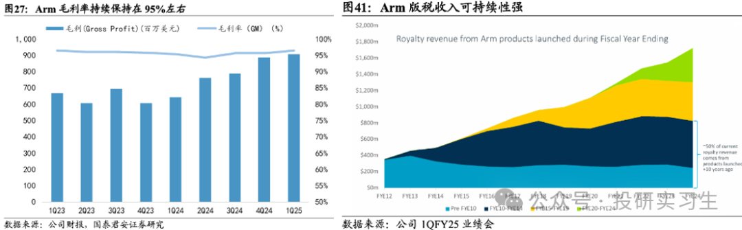
 Thanks to this model of one-time development costs plus marginal costs approaching zero, ARM’s business is highly profitable, with gross margins exceeding 95%. More vividly, ARM continues to earn royalty income from products launched when it was first established in 1990, and IP cores designed by ARM ten years ago still contribute 50% of its royalty income today.
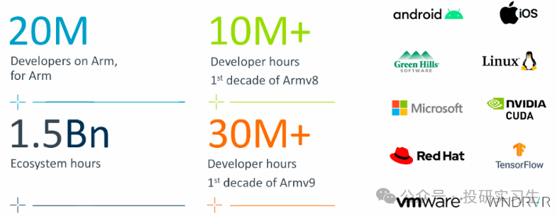
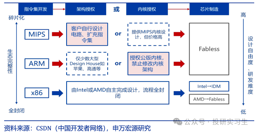
 With the rise of subscription models, ARM has also shifted from the previous one-time TLA and ALA fee structures to new ATA and AFA subscription fee models. Specifically, ARM’s products licensed to customers include instruction set architectures and the aforementioned soft cores, firm cores, and hard cores.At the instruction set architecture level, ARM’s architecture licensing is generally cheaper than core licensing, allowing chip design companies to fully customize their chips according to their needs, but this requires strong design capabilities, and only companies like Apple, Qualcomm, and NVIDIA utilize it. ARM’s strategy has successfully attracted a large number of customers, helping it build a complete ecosystem.
 In contrast, the MIPS architecture has set its architecture licensing prices higher than core licensing to encourage independent development, resulting in fewer customers and failing to build an effective ecosystem, while x86 is a completely closed ecosystem dominated by Intel and AMD.
 In the past, TLA (Technology Licensing Agreements) targeted various IP core licenses, with specific soft, firm, or hard cores determined through negotiation, where customers paid a high one-time licensing fee. ALA (Architecture Licensing Agreements) targeted ARM instruction set architecture licensing, offering high flexibility but with a high technical threshold.
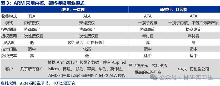 Under the newly implemented subscription model, ATA (ARM Total Access) targets a basket of IP core licenses, available on an annual subscription basis. AFA (ARM Flexible Access) allows for more flexible adjustments to the range of IP cores licensed, also on an annual subscription basis, making it more suitable for small and medium-sized companies. Additionally, under the AFA model, ARM will charge a licensing fee for each product included in the design before the chip design is completed and put into production.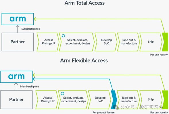
3. Industry Landscape
The Chinese semiconductor IP market is still in its early development stage, with the market size expected to reach 19.9 billion yuan by 2025, and a CAGR of 20% from 2018 to 2025.
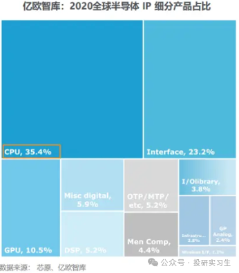
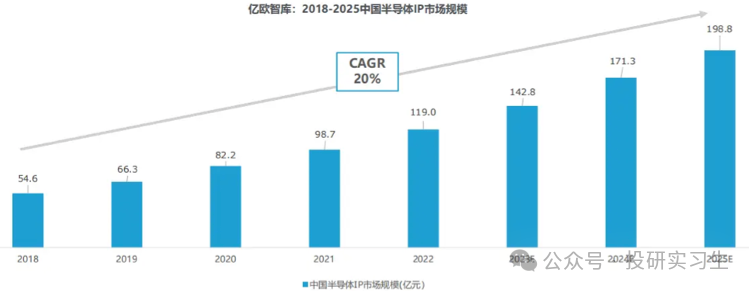 In terms of market share by segment, processor IP is the largest track, accounting for about 49.5%, including CPU, GPU, NPU, VPU, DSP, and ISP. The second largest is interface IP, accounting for 24.9%, of which 95% are wired interface IP (PCIe, DDR, D2D, SerDes, USB). Finally, there are other physical IPs.
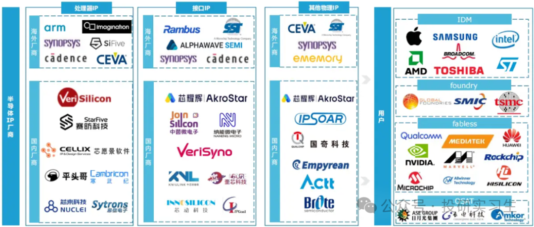
 In the most valuable processor IP track, representative companies include ARM, Synopsys, and Cadence. Domestic companies are mostly lagging behind foreign companies, but both Cambricon, which has recently gained popularity due to its partnership with large AI companies like DeepSeek, and Chipone, whose NPU is used in Xiaomi’s Xuanjie O1, are catching up.
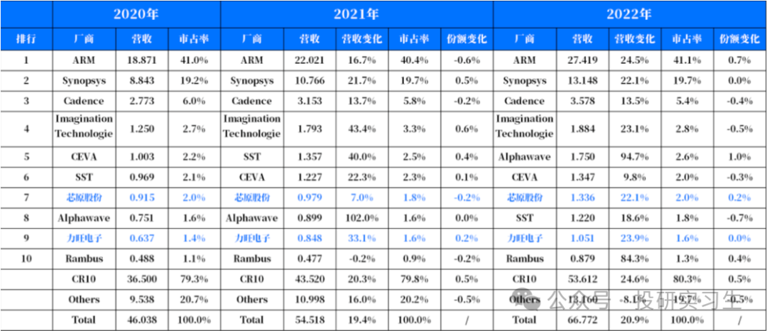
 From a global market share perspective, ARM holds the top position with a 41% market share, followed by Synopsys and Cadence. Among domestic companies, only Chipone and Lianwang Electronics made it to the top ten, with market shares of 2% and 1.6%, respectively.
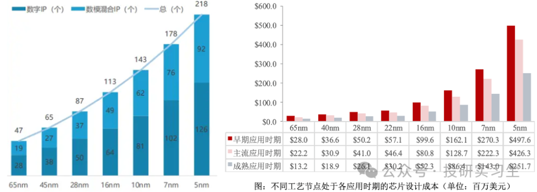
 The IP core industry benefits from the increased complexity brought about by advancements in chip processes. As processes reach 7nm, 5nm, and 3nm, design costs have risen sharply, making reusable IP cores both cost-effective and convenient for chip design teams, thus leading to increased usage of IP cores.
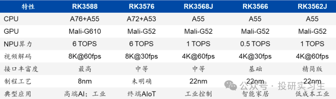
 Currently, the mobile processor market is dominated by the ARM architecture, with its market share in smartphone SoCs exceeding 90%. ARM’s instruction set architecture and its various forms of IP cores are widely used in various mobile terminal devices.For example, the flagship product RK3588 from domestic leading SoC design company Rockchip uses ARM’s mature CPU and GPU IP cores along with its self-developed NPU: including high-performance Cortex-A76 cores, energy-efficient Cortex-A55 cores, and Mali-G610 GPU.
 Other similar companies in China include Huawei, Chipone, and other industry leaders, with Huawei’s Kirin Kunpeng series chips relying on the ARM instruction set architecture.
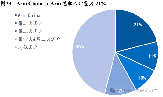
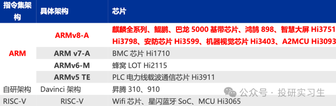 This ARM IP + self-developed acceleration unit model has become the mainstream strategy in the industry: manufacturers leverage the ARM ecosystem to ensure compatibility and development efficiency while achieving differentiated competition through self-developed NPUs, ISPs, and other key units. According to Q1 2025 data, ARM’s revenue contribution in the Chinese market (operated through ARM China) reached 21%, highlighting its significance.
 However, the high licensing fees of ARM have also sparked industry controversy, and under the strategic need for core technology autonomy, domestic companies are actively seeking alternatives. Among them, the open-source and free RISC-V instruction set architecture, with its modular design, customizable features, and advantages of not being subject to export controls, is becoming the most promising alternative.In 2010, a research team from the University of California first introduced the fifth generation of the RISC instruction set—RISC-V. Although RISC-V and ARM belong to the same RISC instruction set family, RISC-V features complete open-source, a more streamlined instruction set, and support for modular development, providing customers with low-cost and more flexible options.The ecosystem of RISC-V is led by the non-profit RISC-V International Foundation, attracting over 4,000 global members, including Qualcomm, Samsung, Intel, and NVIDIA, to participate in technology development and standard setting.In February of this year, Alibaba held the Xuantie RISC-V ecosystem conference in Beijing, launching the server-grade processor Xuantie C930 and the Wujian 600 development platform, promoting the expansion of RISC-V from the embedded market to high-performance computing fields.On the edge, from major companies like Chipone, Huawei, and Google to startups like Huami, many manufacturers are beginning to use the RISC-V architecture and actively build its ecosystem. In the future, IP cores and chips based on the RISC-V architecture are expected to break ARM’s monopoly and create a new revenue distribution model.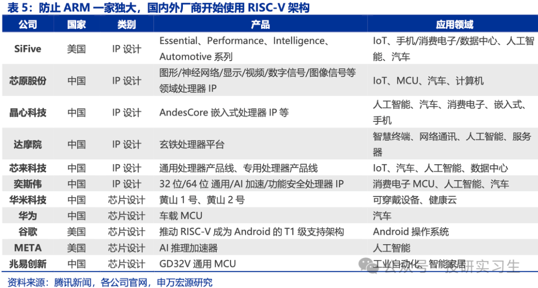
Disclaimer: This article does not constitute investment advice and is for learning and reference only!
References:
· Ping An Securities – AI Industry Series In-Depth Report (5) ~ AI Mobile: The Focus of AI Development Gradually Shifts to the Edge, Apple Expected to Initiate AI Mobile Replacement – 2024/08/23· Guosheng Securities – Rockchip – 603893 – AIoT SoC Platform Layout, Edge AI Trendsetter – 2025/05/11· Guotai Junan – ARM – ARM.US – Initial Coverage Report: The Technological Cornerstone of the AI Era, Leading the Future of Computing – 2024/09/16· Shenwan Hongyuan – Computer Industry Huawei Series Report No. 17: ARM Advantage Fission and AI Opportunity Resonance – 2024/12/30· Guosheng Securities – Chipone – 688521 – The Backbone of Domestic Computing Power, One-Stop Customization & IP Leader – 2025/06/11· Yiou Think Tank – 2023 China Semiconductor IP Industry Research Report· Chipone Prospectus
Welcome to Follow
Investment Research Intern