Abstract: Integrating multiple heterogeneous chiplets into a package is a promising and cost-effective strategy that can build flexible and scalable systems and effectively accelerate diverse workloads. Based on this, we propose Arvon, which integrates a 14nm FPGA chiplet and two closely packed high-performance 22nm DSP chiplets using embedded multi-chip interconnect bridges (EMIBs). The chiplets are interconnected via a 1.536-Tb/s Advanced Interface Bus (AIB) 1.0 interface and a 7.68-Tb/s AIB 2.0 interface. Arvon is programmable and supports a variety of workloads, from neural networks (NN) to communication signal processing. Each DSP chiplet provides a peak performance of 4.14 TFLOPS in half-precision floating-point operations while maintaining an energy efficiency of 1.8 TFLOPS/W. We also developed a compiler that can allocate workloads for FPGA and DSP to optimize system performance and resource utilization. The AIB 2.0 interface implemented with 36-µm-pitch micro-bumps achieves a data transfer rate of 4 Gb/s/pin, with an energy efficiency of 0.10–0.46 pJ/b including the adapter. Its Shoreline bandwidth density reaches 1.024 Tb/s/mm, and areal bandwidth density reaches 1.705 Tb/s/mm².
I. Introduction
With the rapid development of fields such as machine learning, robotics, and 5G/6G communications[1], [2], [3], [4], the DSP workloads for these fields are becoming increasingly dynamic and diverse. A flexible and computationally efficient hardware system can meet these demands well. Such a system can integrate multiple components, including CPUs, FPGAs, and DSP accelerators, where CPUs or FPGAs provide the necessary flexibility, and DSP accelerators provide efficient core acceleration.
One approach to realize such systems is to design and manufacture a monolithic system-on-chip (SoC). However, building a large SoC comes with high time and economic costs. As a cost-effective and feasible alternative, heterogeneous system-level packaging (SiP) with 2.5D or 3D chiplet integration offers a promising path to construct large-scale systems that achieve performance comparable to monolithic integration while avoiding the high costs, risks, and workloads associated with monolithic integration. SiP consists of interconnected components called chiplets. Each chiplet contains a functional module that can be manufactured at the most suitable technology node for optimal performance and efficiency. Since each chiplet is smaller in size and more specialized in function, its design complexity is reduced, and yield is improved. By selecting known good die (KGD) to assemble the SiP, system yield can be enhanced. In the envisioned future chip ecosystem, we can procure verified chips from different suppliers and reuse them when constructing diverse systems, effectively overcoming challenges and obstacles encountered in the rapid development of new systems.
Figure 1 shows a SiP solution for a multifunctional accelerator that integrates an FPGA chiplet, a DSP accelerator chiplet, and possibly additional chiplets such as an analog-to-digital converter (ADC) or optical transceiver. This heterogeneous SiP design can flexibly map various dynamic DSP workloads—from machine learning to communication signal processing—onto it. The FPGA chiplet provides the necessary adaptability, the DSP chiplet contributes efficient computing power, and the additional chiplet provides connectivity to frontend (FE) components such as sensors, wireless, or optical interfaces. Within the SiP, the inter-chip interfaces between chiplets are crucial for data transmission, and they must provide sufficiently high bandwidth to ensure performance comparable to a monolithic SoC while maintaining low energy consumption per bit, ensuring the competitiveness of the entire solution.
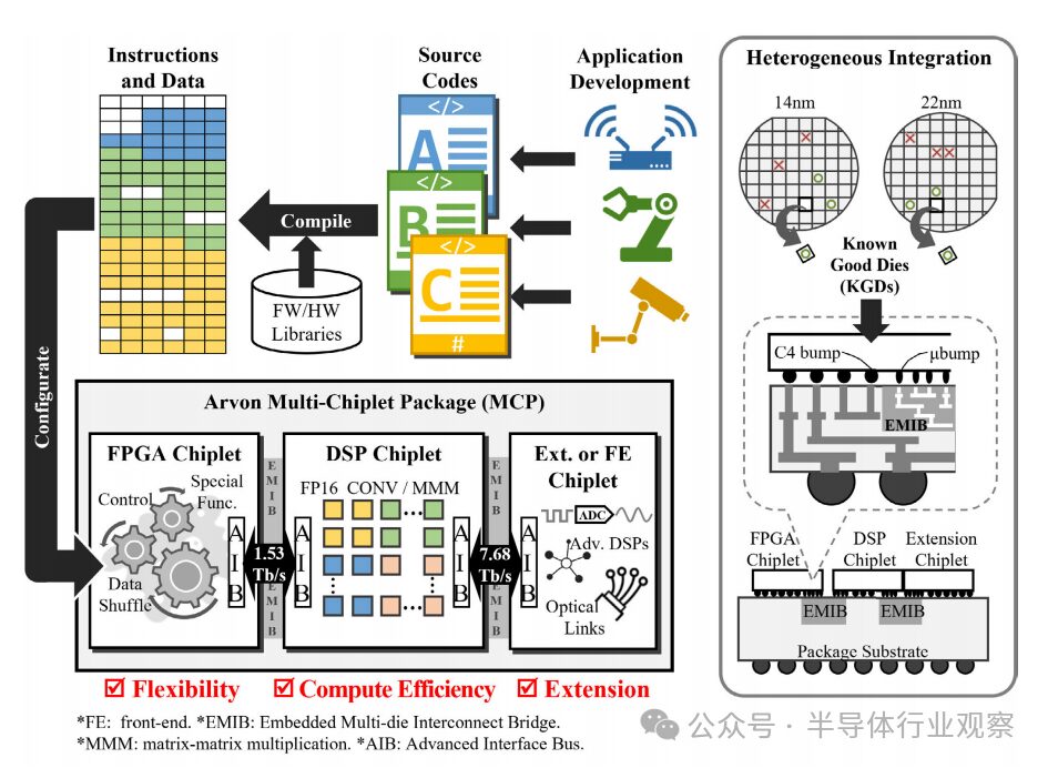
Figure 1 Arvon SiP achieves flexible workload mapping through heterogeneous integration of FPGA, DSP, and FE chiplets
Recent studies have demonstrated the integration of chiplets in SiPs with high bandwidth and efficient die-to-die interfaces[5], [6], [7], [8], [9], [10], [11]. In literature[5], two dual-Arm core chiplets are integrated on chip-on-wafer-on-substrate (CoWoS) with a low-voltage package interconnect (LIPINCON) interface of 8-Gb/s/pin. In literature[6], 36 deep neural network (DNN) accelerator chiplets are integrated on an organic substrate using a ground-referenced signaling (GRS) interface of 25-Gb/s/pin[7]. In literature[8] and[9], four runtime reconfigurable universal digital signal processors (UDSP) are integrated on a silicon interconnect structure (Si-IF) with a 1.1 Gb/s/pin SNR-10 interface. IntAct[10] integrates six 16-core chiplets on an active silicon interconnect layer using a 1.2-Gb/s/pin 3-D-Plug interface. These results represent typical applications of homogeneous integration, effectively scaling computing systems by stitching together multiple instances of modular chiplets.
In Arvon, we demonstrate heterogeneous integration of different types of chiplets to build a multifunctional accelerator for DSP workloads. Arvon consists of a 14nm FPGA chiplet and two 22nm DSP chiplets integrated through embedded multi-chip interconnect bridge (EMIB) technology[12], [13]. We prototyped the first-generation and second-generation open advanced interface bus (AIB) inter-chip interfaces, named AIB 1.0 and AIB 2.0, respectively, to connect these chiplets. The results are demonstrated in a SiP that can effectively accelerate various machine learning and communication DSP workloads while maintaining high hardware utilization. This work also showcases the AIB 2.0 interface, which achieves a coastline bandwidth density of 1 Tb/s/mm with an energy efficiency of 0.1 pJ/b.
The remainder of this paper is organized as follows: Section II provides an overview of the Arvon SiP. Section III elaborates on the design of the AIB interface, including physical layer (PHY) I/O, clock distribution, and bus adaptation. Section IV delves into the details of the DSP chiplets and their vector engine design. Section V discusses the mapping of various workloads. Section VI introduces chip measurements and system evaluation. Finally, Section VII concludes the paper.
II. ARVON SYSTEM OVERVIEW
The overview of the Arvon system is shown in Figure 2. The system consists of one FPGA chiplet and two DSP chiplet instances, named DSP1 and DSP2, respectively. DSP2 is a physical rotated version of DSP1. The FPGA connects to DSP1 using AIB 1.0 interface through EMIB technology, while DSP1 connects to DSP2 using AIB 2.0 interface through EMIB technology. Arvon provides three operational modes, as shown in Figure 2. In modes 1 and 2, the FPGA connects to either DSP1 or DSP2 and offloads general computing cores onto the DSPs. These general cores include matrix multiplication (MMM) and two-dimensional convolution (conv), which are critical in neural network (NN) and communication workloads. In mode 3, DSP1 and DSP2 are combined to enhance computational capacity. DSP2 can also be replaced by an FE chiplet (for example, optical tile or ADC tile) to realize a complete communication or sensing system.
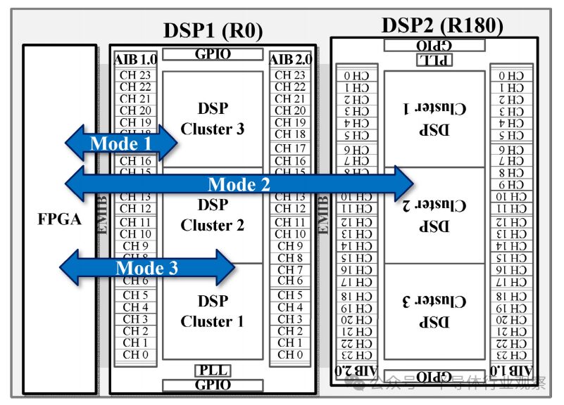
Figure 2 Data flow modes supported by Arvon SiP: In modes 1 and 2, the FPGA connects to one of the DSPs; in mode 3, the FPGA connects to both DSPs simultaneously
A
DSP Chiplet
The DSP chiplet provides offloading and acceleration capabilities for compute-intensive workloads. The design of the chiplet is illustrated in Figure 2. The chiplet has inter-chip interfaces placed on both sides. On the west side, there are 24 AIB 1.0 interface channels, providing 1.536 Tb/s bandwidth for communication with the FPGA. On the east side, there are 24 AIB 2.0 interface channels, providing 7.68 Tb/s bandwidth for communication with another DSP. The chiplet contains three DSP clusters, each providing 1024 16-bit half-precision floating-point processing elements (PE). Each cluster can use up to 8 AIB 1.0 interface channels and 8 AIB 2.0 interface channels for input and output. A low-jitter ring oscillator (PLL) generates clocks for the DSP clusters and AIB 1.0 and AIB 2.0 interfaces. There are two rows of general-purpose input/output (GPIO) ports along the top and bottom of the chiplet for global configuration and debugging.
B
FPGA Host Chiplet
The FPGA plays a key role in realizing the flexibility of Arvon. The programmable logic of the FPGA is used to support various tasks, such as transposing and shuffling data for the DSP. Additionally, the FPGA can provide special functionalities that are not available on the DSP, thus meeting complete processing requirements.
In Arvon, the FPGA acts as the host, taking the form of an instruction-based processor as shown in Figure 3. A simple host processor is equipped with instruction memory, data memory for storing input/output data and weight data, and a direct memory access (DMA) unit for managing and coordinating data transfers with DSP chiplets. The instructions are used to configure and reconfigure the DSP at runtime, guide the data flow between data memory and DSP, and execute preprocessing and postprocessing for the DSP.
When the host processor within the FPGA triggers and reads the first instruction from the instruction memory, the execution of the workload officially begins. These instructions detail all the necessary information, including data content, register access addresses, memory addresses, bus addresses, data lengths for DMA read/write operations, and execution order. According to the instructions, the host processor generates AXI bus transactions to access the DSP configuration registers sent to the DSP. At the same time, it also issues DMA commands to read or write data from the data memory and to read and write data to the DSP. Given the fast processing time of the vector engine in the DSP, the FPGA, including the host processor, is highly utilized to minimize latency and prevent any potential bottlenecks.
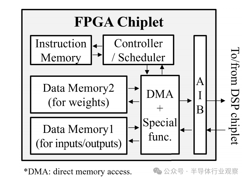
Figure 3 Example of FPGA host implementation
III. AIB Inter-Chip Interface
Within the DSP chiplet, 24 AIB 1.0 interface channels[14] are integrated on the west side, and 24 AIB 2.0 interface channels[14] are integrated on the east side. The AIB channels consist of two layers: an adapter layer and a physical layer I/O layer. The adapter layer is responsible for coordinating data transfers between the DSP core and the physical layer I/O. It handles data framing and synchronization between the two domains. A state machine is used to initiate the AIB link and enable automatic clock phase adjustment. This adjustment helps determine the eye width and center of the data. In AIB 2.0, the adapter also supports optional data bus inversion (DBI), which reduces bus switching activity and improves energy efficiency.
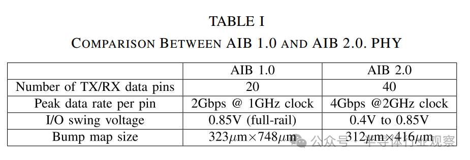
The physical layer implementation of the AIB interface achieves source-synchronous, short-distance, low-latency, and parallel single-ended I/O. In double data rate (DDR) mode, each I/O port of AIB 1.0 provides a bandwidth range from 1 Mb/s to 2 Gb/s through full-track signaling. AIB 2.0 further enhances this by achieving a bandwidth range from 1 Mb/s to 4 Gb/s in DDR mode through a swing change from 0.4 V to full-track signaling, significantly improving data transfer rates. A single AIB 1.0 channel consists of 96 pins, including 2 TX clock pins, 2 RX clock pins, 20 TX data pins, 20 RX data pins, and additional pins for sideband control and redundancy. In contrast, a single AIB 2.0 channel consists of 102 pins, including two TX clock pins, two RX clock pins, 40 TX data pins, 40 RX data pins, and additional pins for sideband control and redundancy. AIB 2.0 improves upon AIB 1.0 by doubling the data transfer rate per pin and the number of data pins per channel, thus quadrupling the data transfer bandwidth. Additionally, AIB 2.0 enhances energy efficiency by using low-swing signaling. A comparison summary of AIB 1.0 and AIB 2.0 is shown in Table I. Notably, AIB 1.0 and AIB 2.0 have similar design structures.
Table I
A
AIB 2.0 Adapter
The AIB adapter manages data transfers between the DSP core and the PHY I/O layer. The data path includes a serializer at the TX end and a parallelizer at the RX end. Figure 4 illustrates a data transmission example. In chiplet 1, an AIB 2.0 TX channel collects four 80-bit wide data streams from the DSP core each time, with the DSP core clock frequency at 500 MHz. The serializer, implemented with a two-stage 2:1 multiplexer, converts the parallel data stream into a single 80-bit wide data stream for transmission. After optional DBI, the 80-bit data is divided into two 40-bit segments, which are sent to the data0 and data1 pins of 40 TX I/O units, respectively. In DDR mode, these TX I/O units operate at a frequency of 2 GHz, with each unit transmitting 2 bits of data at a time, achieving an effective data transfer rate of 4 Gb/s. The differential 2 GHz TX clock is forwarded to chiplet 2 along with the data. In chiplet 2, an AIB 2.0 RX channel is responsible for receiving the 80-bit wide data from 40 RX I/O units. In DDR mode, data is sampled at a frequency of 2 GHz. Subsequently, the received data stream is processed through a parallelizer, which uses a two-stage 1:2 demultiplexer to recover the data into four 80-bit wide data streams. The clock signal from the TX end is fine-tuned through a tunable delay line to meet the sampling clock requirements of the RX end I/O units.
1) Automatic Clock Phase Adjustment: During the initialization phase of the link, the RX clock phase is adjusted to sample the RX data at the optimal point. The adapter employs an automatic RX clock phase adjustment mechanism. The TX is responsible for sending a known pseudo-random binary sequence (PRBS), and the RX utilizes a configurable delay line to scan the delay of the clock signal received from the TX, monitoring potential errors. By analyzing the error patterns in the received PRBS sequence, the RX can estimate the boundaries of the eye diagram. The goal is to set the delay and sampling point at the estimated midpoint of the eye diagram.
2) Data Bus Inversion (DBI): AIB 2.0 supports data bus inversion, which effectively reduces conversion and synchronous switching output (SSO) noise in single-ended and source-synchronous interfaces. Figure 5 shows a 1:19 ratio DBI encoder and decoder. At the TX end, the 80-bit data is encoded by four parallel DBI encoding units. Each unit obtains the values of 19 data lines (represented as icurr[18:0] in Figure 5) and counts the number of bits that have flipped in the previously encoded data (iprev[18:0]). If the count exceeds 10 (half of 20 bits), the DBI encoding unit flips those bits and assigns a high (HIGH) value to the DBI bit. If the count equals 10, and the previous DBI bit is already high (HIGH), the DBI bit remains high (HIGH). If neither condition is met, the data remains unchanged, and the DBI bit is set to low (LOW). The DBI bit is then combined with the encoded 19-bit data, packed into 20 bits of TX data, and sent to the 20 I/O units. At the RX end, four parallel DBI decoding units are employed. If the DBI bit (the highest bit of the received 20-bit data block) is high (HIGH), each unit flips the received 19-bit data bits; if the DBI bit is low (LOW), the data remains unchanged.
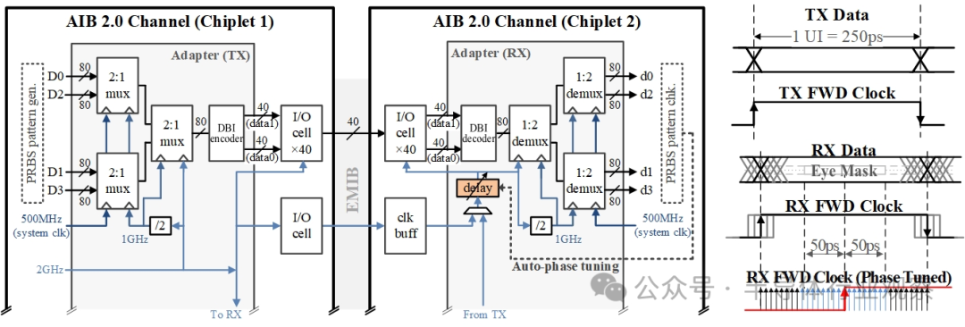
Figure 4 Top-level diagram of AIB 2.0 channel and automatic clock phase adjustment

Figure 5 1:19 ratio DBI encoder (top) and decoder (bottom)
B
AIB 2.0 I/O
Figure 6 illustrates a schematic and layout of a compact unified AIB 2.0 I/O unit design. To achieve the target of 36 µm micro-bump pitch, the layout of this I/O unit has been carefully optimized, with each unit connected under the corresponding micro-bump to ensure the layout meets the specified bump pitch. The unified I/O unit supports multiple modes. First, the transmission direction can be flexibly set to TX or RX mode, which aids redundancy repair and facilitates flexible connections between chiplets. In TX mode, the clock of the RX component is gated to reduce power consumption; conversely, in RX mode, the clock of the TX component is gated. Secondly, for AIB 1.0 and AIB 2.0, the I/O signal swing can be set to full track, while for AIB 2.0, the swing can also be reduced to 0.4 V. Thirdly, the transmission mode can be set to single data rate (SDR) mode or double data rate (DDR) mode. In DDR mode, data0 and data1 are serialized for transmission, with data1 delayed by half a clock cycle compared to data0. This means that on the positive edge of the TX clock, data0 is sent to the driver, while on the negative edge, data1 is sent. At the RX end, this process is reversed, with data restored through parallelization. The SDR mode uses only data0, which is sent to the driver on the positive edge of the TX clock. Finally, the I/O unit can be configured to operate in asynchronous mode with clock and other sideband signals.
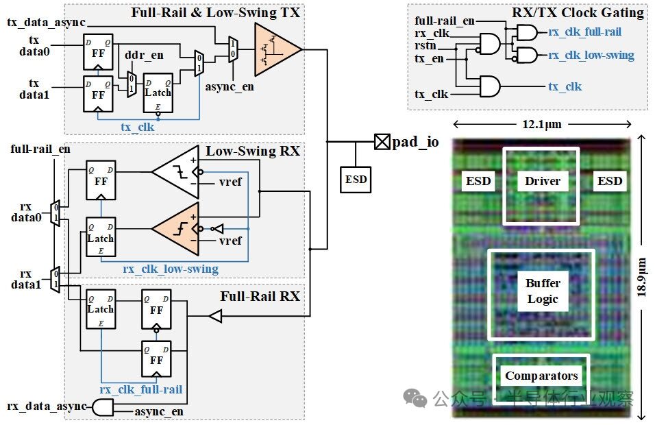
Figure 6 Schematic and layout of a unified AIB I/O unit
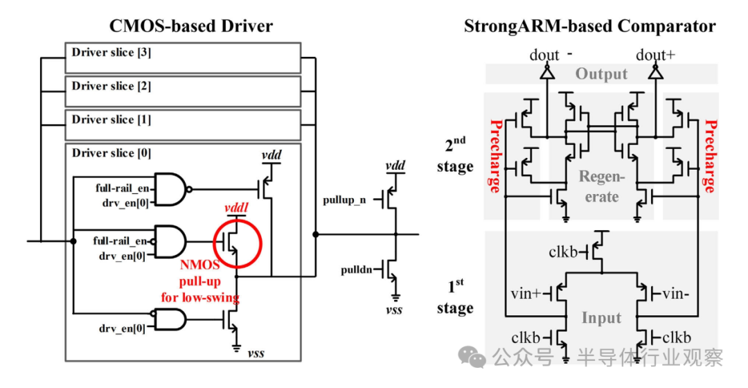
Figure 7 CMOS-based TX driver (left) and strongARM-based RX (right) schematic
1) TX Driver: As shown in Figure 7 (left), the design of the TX driver adopts a segmented technique, consisting of four parts. This design allows up to four segments of drivers to be connected for adjustable driving strength, enabling flexible adjustments based on channel variations while balancing transmission speed and power consumption. Each driver segment includes an NMOS transistor for pull-down, along with a switchable PMOS or NMOS pull-up driver, which can provide full track or low swing driving power as needed. In low-swing mode, the NMOS pull-up driver is moderately enhanced to ensure balance with the pull-down driving power. Additionally, the system allows for initial power-up values to be configured by setting weak pull-ups and pull-downs.
2) RX Buffer: The design of the RX buffer distinguishes between full-track input and low-swing input. For full-track input signals, standard cell buffers are used for processing; for low-swing input signals, a regenerative comparator is employed, as shown in Figure 7 (right). This comparator is an optimized version of the StrongARM latch[15], [16], reducing average offset to 4.1 mV without calibration. Additionally, PMOS is utilized in the design to enhance detection of low-swing inputs. The design employs a simple reference voltage generator. The comparator can reliably detect inputs as low as 0.38 V at a 2 GHz DDR frequency.
3) Bump Map: Figure 8 shows the bump map of an AIB 2.0 channel with a 12×17 bump configuration. This channel consists of 40 TX data pins, 40 RX data pins, 2 TX forwarding clock pins, 2 RX forwarding clock pins, and 18 sideband and redundancy pins. The designs of the TX and RX bumps are symmetrical, ensuring that the wiring lengths for each pair of TX-RX on the EMIB are equal. It has a total of 80 data pins, each with a data rate of 4 Gb/s, providing a total bandwidth of 320 Gb/s for an AIB 2.0 channel. The design has a micro-bump pitch of 36 µm, with a channel shoreline width of 312.08 µm, achieving a bandwidth density of 1024 Gb/s/mm.
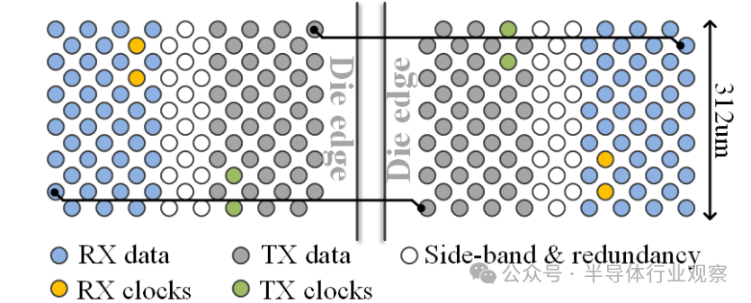
Figure 8 Bump map of an AIB 2.0 channel
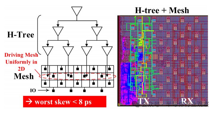
Figure 9 Two-stage clock distribution
C
Clock Distribution
For high-speed parallel I/O interfaces like AIB, low-skew clock distribution must be employed to ensure that all data pins in a given channel are phase-aligned correctly. As shown in Figure 9, we adopt a two-stage clock distribution in each AIB channel. The upper layer is a balanced H-tree structure that covers the entire channel, while the lower layer consists of a local clock grid. This dual-layer design effectively limits the depth of the H-tree, ensuring better balance between branches. Additionally, the local clock grid provides more stable clock sinks without significantly increasing power consumption. Therefore, the entire clock network can control the worst-case clock skew to within 8ps. Both the H-tree and the grid clock network are created and evaluated using the multi-source clock tree synthesis (MSCTS) process of IC Compiler II.
IV. DSP Clusters
As shown in Figure 10, each DSP cluster includes a flexible vector engine, a bypass buffer, a rotation block for data framing, two AXI-compatible bus converters for packing and unpacking data across multiple AIB channels, and an AXI-compatible system bus. Additionally, a bus hub is included to establish connections between the vector engine and the tester, AIB 1.0 interface, or AIB 2.0 interface. The bypass buffer supports mode 2 operation of Arvon, allowing direct connection between the FPGA and DSP2, bypassing DSP1. Through this connection, the AIB 1.0 transactions from the FPGA can be directly forwarded to the AIB 2.0 transactions of DSP2. The rotation block reverses the channel index order of the AIB interface. For example, when connecting DSP1 to DSP2 (the rotated version of DSP1), channels 1-8 of DSP1 connect to channels 24-17 of DSP2, requiring the rotation block of DSP2 to reverse the connection order.
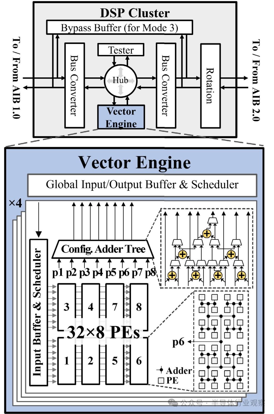
Figure 10 DSP cluster (top) and vector engine (bottom)
A
Vector Engine
The core component of the DSP cluster is the vector engine, which consists of four 2-D symmetric array instances[17]. Each pulsed array contains 256 PEs, with each PE performing multiplication in half-precision floating-point format (FP16). These 256 PEs are divided into eight units, each containing 32 PEs. The summation results of each 32-PE unit are then input into a configurable adder tree. The configurable adder tree can flexibly support various workload mappings by selecting which units among the eight to sum together. This design provides shorter partial summation accumulation paths and achieves higher utilization through concurrent workloads, distinguishing it from classical pulsed arrays. The entire vector engine offers a total of 1024 PEs to support matrix-matrix multiplication (MMM) and convolution (conv). Finally, a global I/O buffer and scheduler are implemented, using multicast or round-robin arbitration techniques to allocate inputs to the PE array.
Through instruction configuration, the vector engine facilitates continuous computation of input streams. The vector engine also features high mapping flexibility. First, the four pulsed arrays can be independently mapped. Furthermore, the 256 PEs within each array can be configured in units of 32 PEs, accommodating from 1 to 8 independent workloads.
B
System Bus and Bus Converter
The AIB connections are abstracted by a point-to-point system bus compatible with AXI. The bus converter handles the packing and unpacking of data across multiple AIB channels. It also supports burst mode to maximize bandwidth for streaming. The channels and signals of the system bus are illustrated in Figure 11. The system bus consists of four channels: read command channel, write command channel, read data channel, and write data channel. A master device can issue a read/write command with a 32-bit address and a 6-bit burst length, along with 512 bits of write data and write commands. In response to a read command, the slave device sends back 512 bits of read data to the master device. The conversion between the system bus and AIB channels is completed by the bus converter. We adopted a header-based streaming method in designing the bus converter to achieve high bandwidth and low latency. A vector engine can utilize up to eight AIB channels to ensure optimal utilization. Each AIB channel can be flexibly configured as a master or slave device, allowing TX/RX bandwidth to be adjusted as needed.
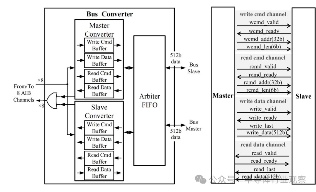
Figure 11 AXI-compatible system bus: bus converter (left) and bus interface channels and signals (right)
V. Workload Mapping
As a multifunctional computing platform, Arvon can support computing tasks of different scales, and the complexity of these tasks can be dynamically adjusted based on requirements during operation. To ensure efficient data processing, a systematic approach must be established to map workloads to optimal hardware configurations and data layouts.
To achieve this goal, we developed a compiler, as shown in Figure 12. Workloads are first divided into several parts, namely parts that use conv cores or MMM cores, or both, which can be directly mapped to the Arvon DSP through appropriate configurations. Additionally, some intermediate steps between computation cores can be executed by the FPGA host. Specifically, the configuration for conv is based on the size of the filter and inputs (R × S × C), while the configuration for MMM is based on the size of the matrices. Subsequently, the conv and MMM cores in the workload will be scheduled and allocated to the vector engine of the Arvon DSP according to established instructions and memory data configurations. This allocation process takes into account multiple key factors, including improving resource utilization, enhancing data reusability, and minimizing end-to-end latency.
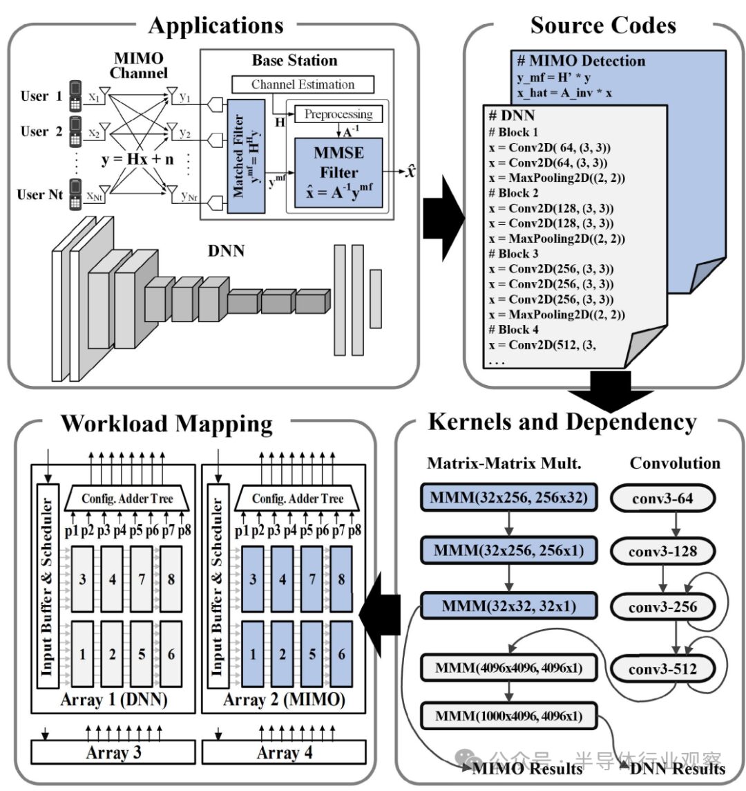
Figure 12 Compiler process for workload mapping
The vector engine adopts a static weight scheme, with its core weights allocated to the PEs. To map MMM onto the vector engine[17], each row of the weight matrix is assigned to a PE, effectively allocating one-dimensional vectors to the two-dimensional array. Rows of the same weight matrix can be assigned to the same group of PEs. In multi-tenant scenarios involving multiple cores, rows of different weight matrices can be assigned to different partitions, represented by p1–p8 in Figures 12 and 13. The partition outputs are directed to the corresponding inputs of the configurable adder tree, ensuring that individual sums are computed as outputs.
The weight mapping for conv is similar to the multi-tenant MMM scenario, as it may involve multiple convolution kernels. Figure 13 illustrates mapping examples for two convolution operations. Each convolution kernel has a size of R × S × C and is unfolded into the two-dimensional PE array by weaving three-dimensional slices in two dimensions. The three-dimensional input activation elements under the sliding convolution window are also unfolded into the two-dimensional PE array accordingly. Input activations are retained within the PE array to achieve horizontal and/or vertical reuse through pulsed data forwarding between adjacent PEs. For the case of a single convolution kernel (as shown in the first example in Figure 13), mapping can be done without considering partition boundaries, achieving efficient utilization. However, when multiple convolution kernels are present, as in the second example in Figure 13, each convolution kernel needs to align with partition boundaries, reducing utilization.
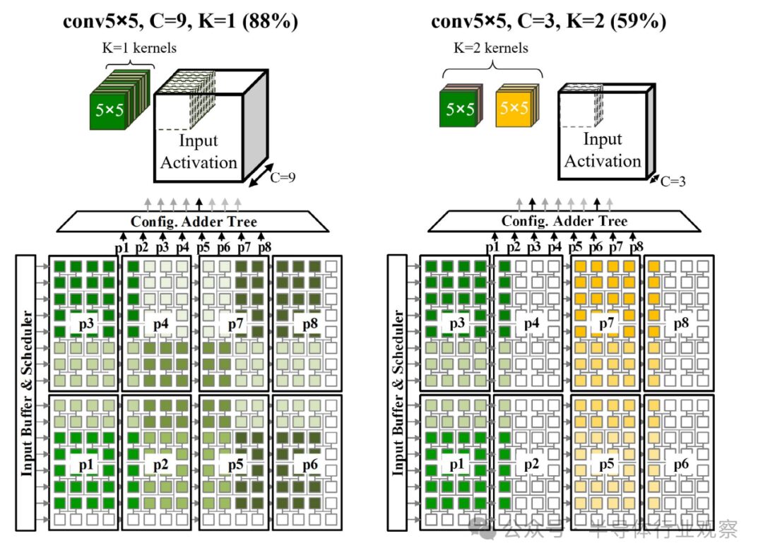
Figure 13 Mapping examples for different kernel sizes
VI. Chip Measurements and Comparisons
The DSP chiplet is manufactured using 22 nm FinFET technology, with an area of 32.3 mm², as shown in Figure 14. To construct the Arvon SiP, we package and interconnect a 14 nm FPGA chiplet and two DSP chiplets using two ten-layer EMIBs, while employing 36 micron pitch micro-bumps. The average wire length on the AIB 1.0 side is 1.5 mm, while the average wire length on the AIB 2.0 side is 0.85 mm.
At room temperature and a chip voltage of 0.85 V, the maximum operating frequency of each DSP cluster is 675 MHz, with a power consumption of 0.76 W. In this configuration, the peak performance of the DSP chiplet is 4.14 TFLOPS, with a power efficiency of 1.8 TFLOPS/W. Under 0.85 V I/O voltage and an 800-MHz clock (limited by the FPGA clock frequency), the power consumption of the AIB 1.0 I/O is 0.44 pJ/b, including the adapter at 0.85 pJ/b, with a transmission delay of 3.75 ns. At room temperature, with an input/output voltage of 0.4 V and a clock frequency of 2 GHz, the AIB 2.0 input/output consumes 0.10 pJ/b, including the adapter at 0.46 pJ/b, with a transmission delay of 1.5 ns. The energy consumption breakdown for the AIB 2.0 interface is shown in Figure 15. The energy consumption of the adapter accounts for the majority at 0.32 pJ/b, approximately 69% of the total energy consumption. On the other hand, the I/O unit consumes only 0.10 pJ/b, accounting for approximately 22% of the total energy consumption. The low energy consumption of the I/O unit is attributed to the utilization of a low signal swing of 0.4 V.
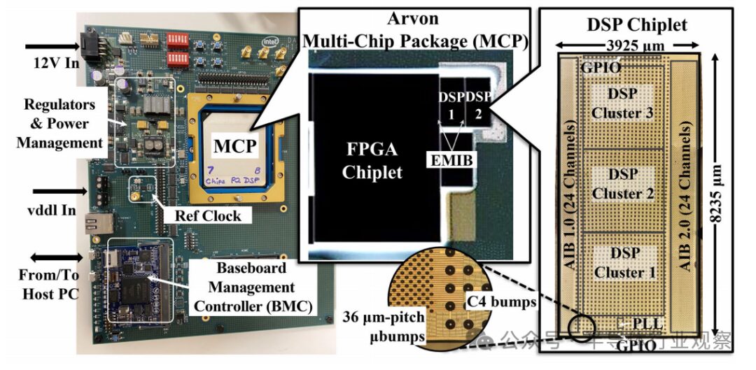
Figure 14 Testing device, Arvon multi-chip package, and microphotograph of DSP chiplet
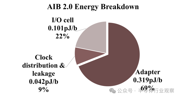
Figure 15 Energy consumption breakdown of AIB 2.0 interface
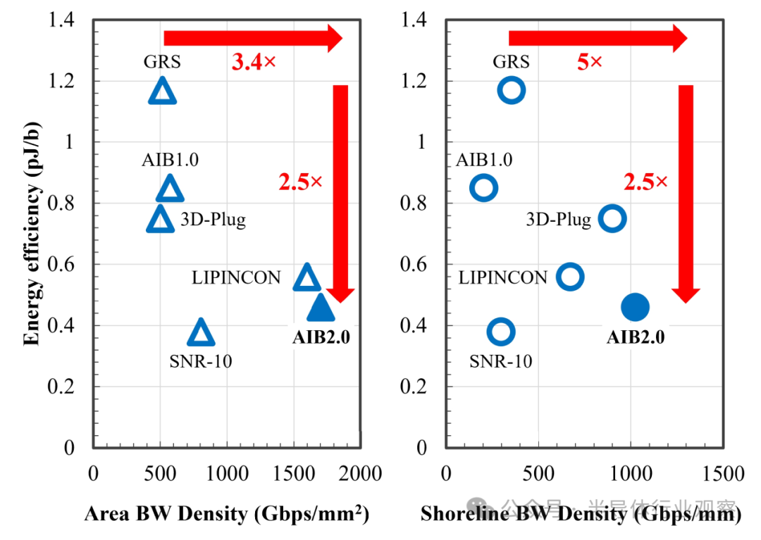
Figure 16 Relationship between energy efficiency and area bandwidth density (left) and shoreline bandwidth density (right)
A comparison of the AIB I/O interface of Arvon with state-of-the-art SiP I/O interfaces is shown in Table II. Similar to the AIB interface, SNR-10[8], 3-D-Plug[10], and LIPINCON[5] are also parallel I/O interfaces. Among them, LIPINCON has the highest data transfer rate, reaching 8 Gb/s/pin, with the lowest I/O energy consumption at only 0.073 pJ/b under a 0.3 V signal swing; 3-D-Plug has the highest bandwidth density, reaching 900 Gb/s/mm shoreline; and SNR-10 has the smallest I/O size, only 137 µm². GRS[7] is a high-speed serial I/O interface that provides 25 Gb/s/pin with an energy efficiency of 1.17 pJ/b. Our AIB 2.0 prototype provides an attractive solution with an I/O energy consumption of only 0.10 pJ/b, including the adapter at 0.46 pJ/b. As shown in Table II, it also achieves the highest bandwidth density of 1.0-Tb/s/mm shoreline and 1.7-Tb/s/mm² area. Figure 16 compares the energy efficiency, area bandwidth density, and shoreline bandwidth density of inter-chip interfaces. Compared to the GRS interface, the AIB 2.0 interface improves energy efficiency, area bandwidth density, and shoreline bandwidth density by 2.5 times, 3.4 times, and 5 times, respectively, outperforming other interfaces.
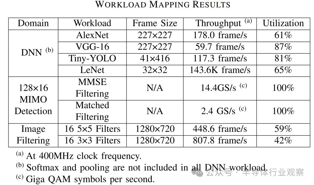
We demonstrate various applications of workload mapping that can leverage Arvon, including deep neural networks (DNN), multiple input multiple output (MIMO) signal processing, and image filtering. The workload sizes, overall throughput, and utilization are summarized in Table III. Besides the commonly used DNN models, the 128×16 MIMO detection workload utilizes 128 receiving antennas to detect 16 single-antenna users. The processing involved includes minimum mean square error (MMSE) filtering operations, which require matrix-matrix multiplication (MMM) calculations to compute the filtering matrix, followed by applying the filtering matrix using MMM. To perform these operations, MMM kernels sized 32×256, 256×32, 32×32, and 32×1 are needed to complete this workload. These computation kernels can be efficiently mapped to the PE array, achieving 100% utilization. The image filtering workload involves 16 5×5 filters and 16 3×3 filters, which are applied to 1280×720 image frames, and these operations require convolution kernels. However, due to the small size of the filters, their utilization is lower than that of other workloads. The results of these example workloads indicate that the heterogeneous SiP architecture of Arvon provides flexibility, performance, and efficiency for neural network (NN) and communication processing.
Table II
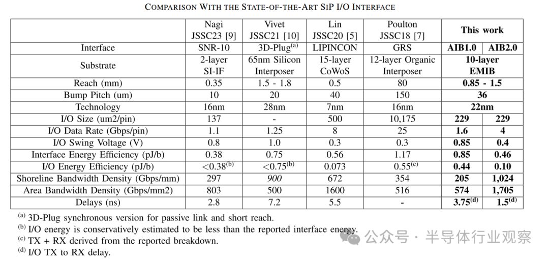
Table III
VII. Conclusion
Arvon is a heterogeneous system-level package (SiP) that integrates an FPGA chiplet and two DSP chiplets using embedded multi-chip interconnect bridges (EMIBs). This integration allows Arvon to leverage the flexibility of the FPGA as a host, while also benefiting from the high computational performance and efficiency of the DSP.
The main features of the SiP include the parallel, short-distance AIB 1.0 and AIB 2.0 interfaces for seamless chiplet connections. The input/output (I/O) unit design is compact and digital-centric, and can be integrated. These units are highly flexible, supporting multiple modes. Furthermore, they employ dependent-mode power gating and two-stage clock distribution, enhancing energy efficiency. We achieved a low-swing 4-Gb/s AIB 2.0 interface with an energy efficiency of 0.10 pJ/b, and 0.46 pJ/b including the adapter, while achieving a shoreline bandwidth density of 1.024-Tb/s/mm and an area bandwidth density of 1.705-Tb/s/mm². The interface abstracts using an AXI-compatible bus protocol, simplifying the usage between the host and DSP.
Each DSP chiplet in Arvon adopts a low-latency pulsed array architecture, featuring 3072 FP16 PEs. These PEs are hierarchically organized into three clusters, with each cluster containing eight 32-PE units. This fine-grained organization allows for the simultaneous parallel execution of multiple workloads. Each DSP chiplet can provide a peak performance of 4.14 TFLOPS with a power efficiency of 1.8 TFLOPS/W. We developed a systematic program for mapping workloads onto Arvon and demonstrated various workloads that Arvon can accelerate to achieve competitive performance and utilization.
Acknowledgments
The views, opinions, and/or findings expressed are those of the authors and should not be interpreted as representing the official views or policies of the Department of Defense or the U.S. government.
Thanks to Professor Huang Letian and student Chen Feiyang from the School of Integrated Circuit Science and Engineering at the University of Electronic Science and Technology of China for their assistance in translation and proofreading.
References
[1] W. Jiang, B. Han, M. A. Habibi, and H. D. Schotten, “The road towards 6G: A comprehensive survey,” IEEE Open J. Commun. Soc., vol. 2, pp. 334–366, 2021.
[2] H. Tataria, M. Shafi, A. F. Molisch, M. Dohler, H. Sjöland, and F. Tufvesson, “6G wireless systems: Vision, requirements, challenges, insights, and opportunities,” Proc. IEEE, vol. 109, no. 7, pp. 1166–1199, Jul. 2021.
[3] S. Bianco, R. Cadene, L. Celona, and P. Napoletano, “Benchmark analysis of representative deep neural network architectures,” IEEE Access, vol. 6, pp. 64270–