8051 Microcontroller Pin Diagram and Function Introduction
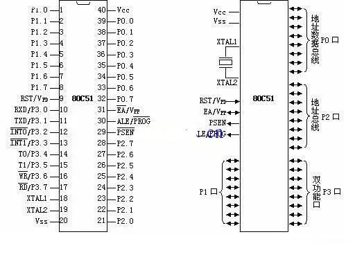
Microcontroller Pin Diagram
The 40 pins can be roughly divided into four categories based on their functions: power, clock, control, and I/O pins.
⒈ Power:
⑴ VCC – Chip power supply, connect to +5V;
⑵ VSS – Ground terminal;
Note: When testing the microcontroller pin current with a multimeter, it is generally 0V or 5V, which is the standard TTL level. However, sometimes when the microcontroller program is running, the test result may not be this value but rather between 0V-5V. This is simply because the multimeter does not respond quickly enough; at a certain instant, the microcontroller pin current still maintains at 0V or 5V.
⒉ Clock: XTAL1, XTAL2 – Inverting input and output terminals of the crystal oscillator circuit.
⒊ Control Lines: There are a total of 4 control lines,
⑴ ALE/PROG: Address latch enable / on-chip EPROM programming pulse.
① ALE Function: Used to latch the low 8 bits of the address sent from port P0.
② PROG Function: For chips with on-chip EPROM, this pin inputs the programming pulse during EPROM programming.
⑵ PSEN: External ROM read selection signal.
⑶ RST/VPD: Reset / Backup power.
① RST (Reset) Function: Reset signal input terminal.
② VPD Function: Connects to backup power in case of Vcc power failure.
⑷ EA/Vpp: Internal and external ROM selection / on-chip EPROM programming power.
① EA Function: Internal and external ROM selection terminal.
② Vpp Function: For chips with on-chip EPROM, applies programming power Vpp during EPROM programming.
⒋ I/O Lines
The 80C51 has 4 parallel 8-bit I/O ports: P0, P1, P2, P3, totaling 32 pins.
Port P3 also has secondary functions for special signal input/output and control signals (part of the control bus).