Chip tape out (Tape Out) is the core step in transforming integrated circuit design into physical chips, involving design verification, process manufacturing, and sample testing, which directly determines the success rate of chip mass production.
The name originates from the early tradition of “streaming” design drawings to magnetic tapes, which has now evolved into the entire process of delivering GDSII layout data to wafer fabs. The cost of a single tape out can exceed $150 million (for 3nm process), taking 4-6 months, making it one of the most expensive “trial and error experiments” in the semiconductor industry.

1. What is Tape Out?
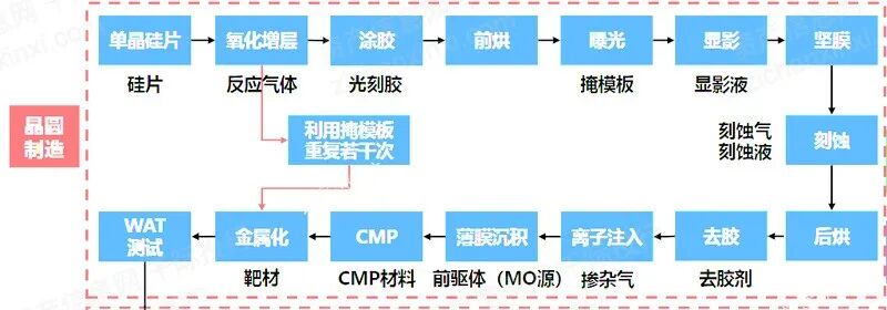
Tape out refers to the manufacturing of chips through a series of process steps on the production line, marking the final stage of integrated circuit design, which is the submission for manufacturing. This process includes precision techniques such as photolithography, etching, ion implantation, and metal deposition, ensuring the accurate construction of the designed integrated circuit on the silicon wafer.
Tape out is essentially a “trial production”; simply put, after completing the circuit design, a few chips are produced for testing. If the tests pass, large-scale production begins based on this design.
Tape out is the process of turning circuit designs into ASIC chips. After a fabless vendor completes the circuit design and verifies that all checks are correct, the final GDSII file is submitted to the foundry to produce a small batch of sample chips (usually several dozen to hundreds) to verify the feasibility of each process step and whether the circuit meets the required performance and functionality.
Essence
Tape out involves delivering the designed GDSII file to the wafer fab, where sample chips (usually dozens to hundreds) are manufactured through photolithography, etching, and ion implantation to verify design feasibility and performance.
Goal: To verify circuit functionality and process compatibility, paving the way for mass production.
Risk: Failure can lead to millions of dollars in losses, and startups may go bankrupt after 1-2 failures.
Value
Design verification: Exposing physical defects not covered by simulations (such as timing deviations and abnormal power consumption).
Precursor to mass production: Optimizing yield through sample testing to avoid risks in large-scale production.
Technical closure: Engineers complete the full process capability loop of “design-manufacture-test” through tape out.

2. Tape Out Methods
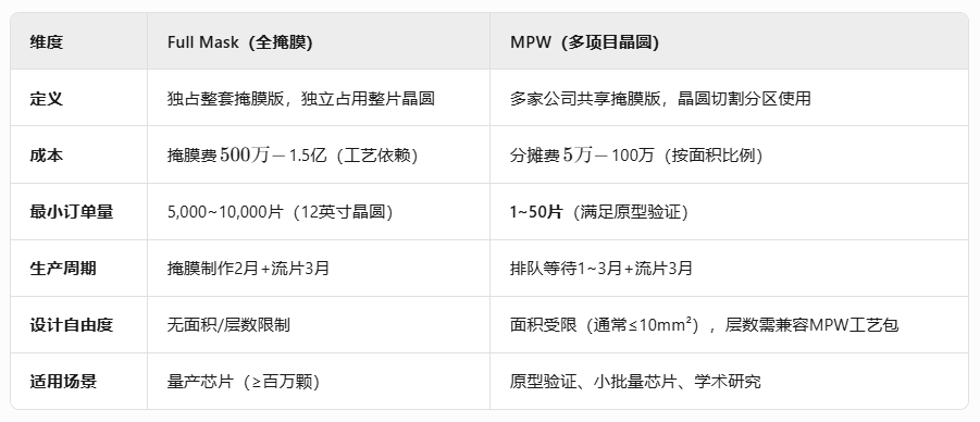
Fabless designers typically deliver the final results of integrated circuit designs in GDSII format to the foundry, a process known as Tape Out. Full Mask and MPW are both methods of tape out (submitting design results for production).
1. Full Mask
A method of tape out, “Full Mask” means that the entire mask in a single manufacturing process is dedicated to a specific chip design.
2. MPW
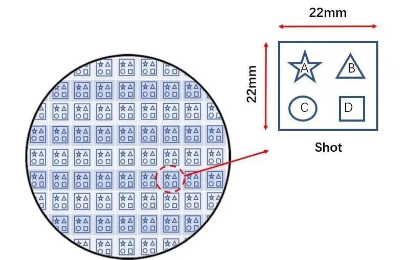
A method of tape out, MPW stands for Multi Project Wafer, which differs from Full Mask in that the entire mask in a single manufacturing process serves multiple chip design projects, allowing multiple IC designs to be manufactured in the same process.
Advantages and Disadvantages
Full Mask means that all masks in the wafer manufacturing process are used for a specific chip, resulting in high tape out costs. It is only adopted when there is complete confidence in success and readiness for mass production, as bulk production can reduce costs.
MPW costs only 5%-10% of the cost of standalone prototype manufacturing, significantly reducing product development risks. However, MPW has a specific process, usually organized by the foundry or third-party service providers, with predetermined MPW time points for various processes within a year, creating some pressure on participants regarding design and development timelines.
MPW shares a mask template with other manufacturers, while FULL MASK has a dedicated mask. If the chip risk is high, MPW can be done first, and if testing is successful, then proceed with FULL MASK.
3. Processes and Key Technologies
1. Mask Production (Core Cost)
The mask, also known as photomask, is a tool for graphic transfer in microelectronics manufacturing, serving as a carrier of graphic design and process technology intellectual property information.
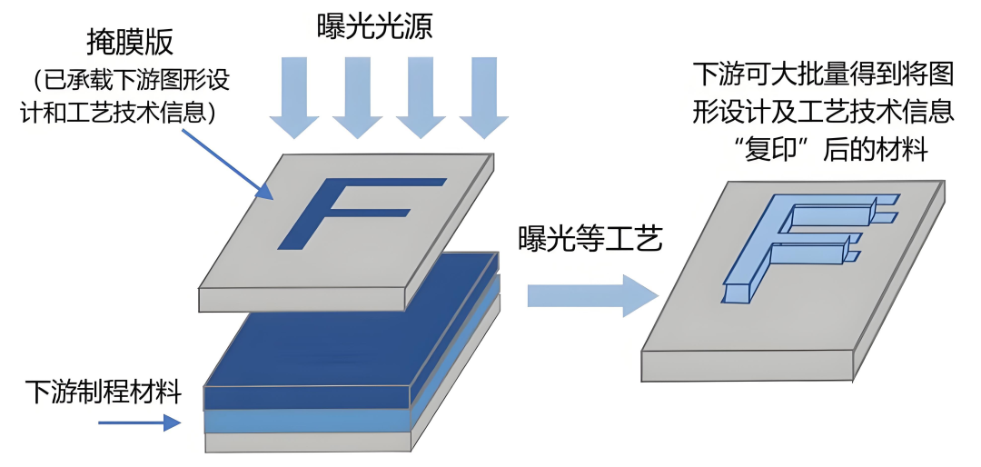
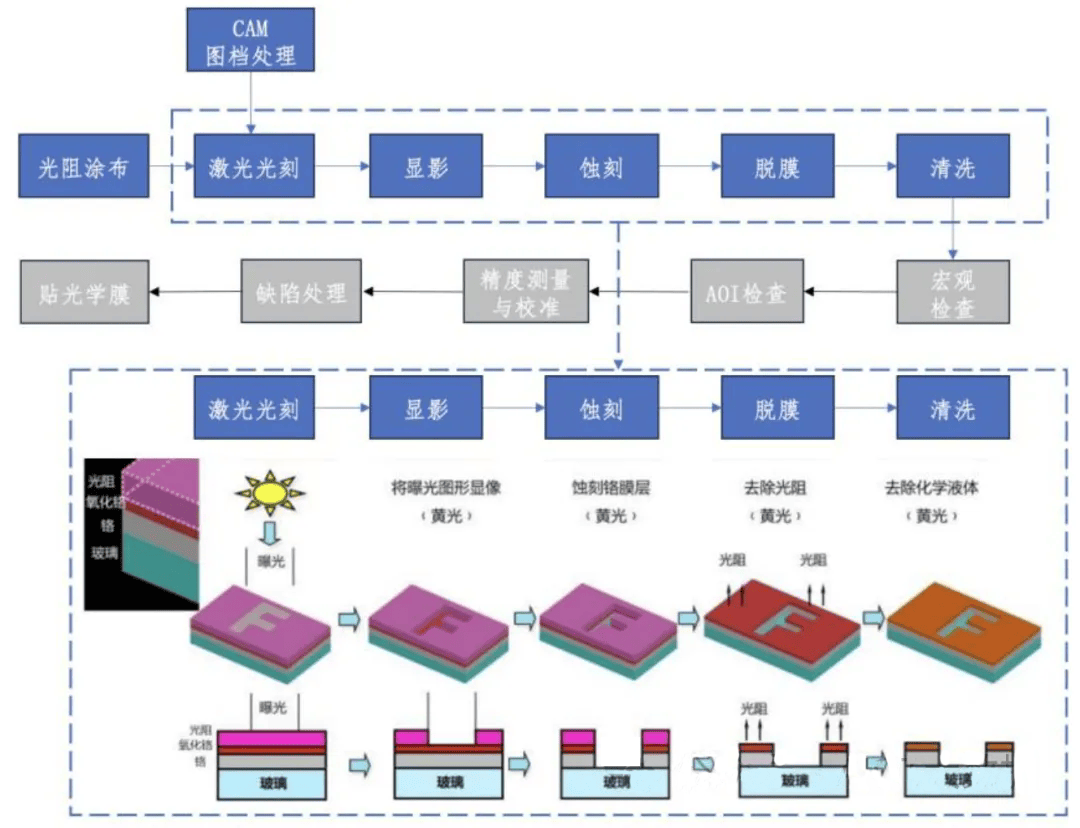
Based on the required graphics, mask manufacturers use photolithography to engrave micron and nanometer-level fine patterns onto the mask substrate (the raw material for the mask is a photosensitive blank board for creating fine photomask graphics), and then wash away the unnecessary metal and glue layers to obtain the finished mask. The role of the mask in downstream production lines is primarily to replicate images (circuit graphics) using the designed patterns on the mask through transparent and opaque methods, thus achieving mass production.
As the benchmark and blueprint for photolithographic graphic replication, the mask is key to connecting industrial design and process manufacturing. The precision and quality level of the mask directly affect the yield of the final downstream products.
The function of the mask is similar to that of a traditional camera’s “film”: transferring the designer’s circuit graphics to the downstream industry’s substrate or wafer through exposure, thus enabling mass production. As the benchmark and blueprint for photolithographic graphic replication, the mask is key to connecting industrial design and process manufacturing, and its precision and quality level directly affect the yield of the final downstream products. The mask is a critical consumable in the photolithography process, as important as the photolithography machine and photoresist.
The “film” of the photolithography process, 7nm processes require over 80 layers of masks, accounting for 60%-70% of tape out costs.
Price examples: 40nm approximately 5 million, 14nm over 25 million.
2. Key Processes in Wafer Manufacturing
Photolithography:
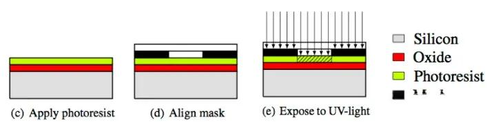
DUV/EUV technology transfers circuit graphics to silicon wafers with nanometer-level precision. A layer of photoresist is applied to the wafer, generally, when exposed to light, the photoresist dissolves (positive resist). Then, the prepared mask is used to expose the wafer.

The cross-section diagram below shows the yellow photoresist we added. The black part is the template made according to the layout. Then, UV light is used to expose and hollow out the photoresist.
Etching and Ion Implantation:
Using chemicals to etch the oxide, then washing off the photoresist, and finally implanting ions. This adjusts the conductivity of the silicon wafer, forming transistors.
Metalization:
This step primarily involves connecting metal lines on the silicon wafer. The process is clearer in the cross-section diagram below. Copper/aluminum lines are deposited to construct circuit interconnections.
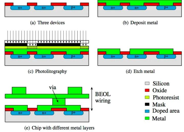
In diagram b, a layer of metal is first plated on top, diagram c uses photoresist and a mask to etch again to obtain diagram d, then layers are stacked through etching, with only fixed vias connecting each layer.
3. Testing and Packaging
WAT (Wafer Acceptance Test), this primarily tests whether the electrical characteristics of the wafer are normal. WAT testing is directly incorporated into the wafer during tape out, mainly including various transistor parameters such as threshold voltage, leakage current, resistance, and capacitance. Generally, the WAT test vectors are provided by the foundry itself.
CP (Chip Probing) testing. After WAT testing passes, the next step is CP testing, where probes are used to check if the chips are good; defective chips are discarded to avoid wasting packaging costs. Generally, the DFT three axes discussed in previous articles are used: scan chain, JTAG, BIST. CP test vectors are provided by the designer. If CP fails, the defective chips are marked and discarded.
CP testing (wafer testing): filters out defective bare chips, and yield determines economic benefits.
After CP testing, the chips are cut into individual small chips along the scribe lines, packaged, and sent out for final testing/packaging.
Packaging: Ceramic/plastic packaging protects the chip and supports board-level integration.
4. Composition of Tape Out Costs and Optimization Strategies
In-depth analysis of tape out costs (using 5nm chips as an example)
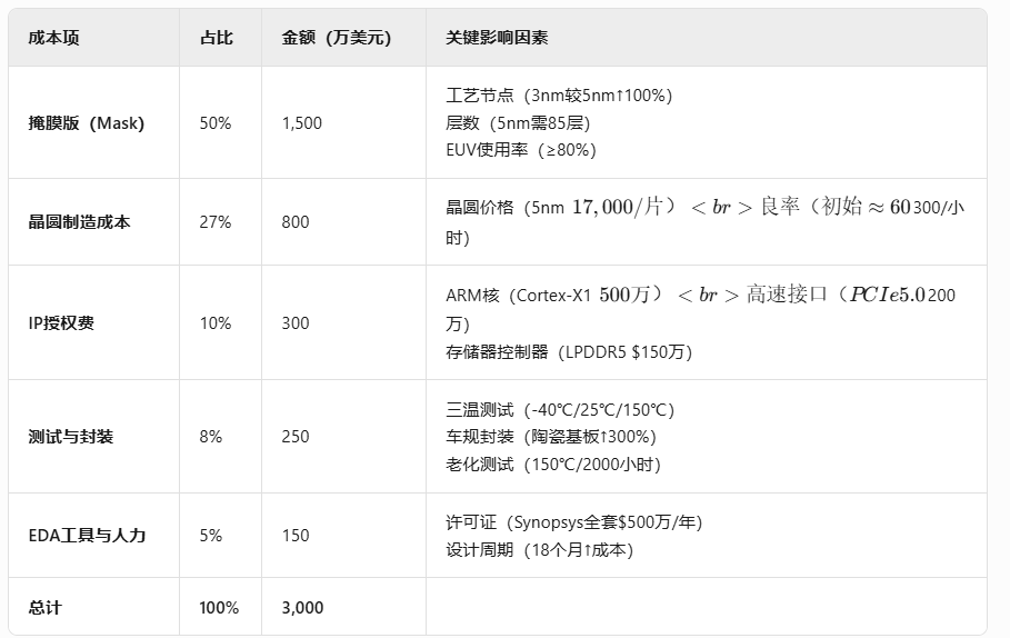
Cost optimization strategies:
1) MPW (Multi Project Wafer) sharing;
2) Wafer size game, 12-inch vs 8-inch wafers;
3) Open-source IP alternatives, IPreuse strategies;
4) Improve tape out yield levels, using mature processes, etc.
5. Why are Tape Out Costs So High?
The price of a single tape out is primarily composed of the costs of the mask and wafer, with the mask accounting for a significant portion.
The mask (Photomask), also known as a photomask, is the graphic master used in the photolithography process of microelectronics manufacturing. The process of transferring graphics from the mask to the wafer is akin to the operation of a banknote printing machine. We can imagine the photolithography machine as a banknote printing machine, where the process of printing the graphics of the banknote master onto paper is similar to how the photolithography machine prints chip graphics onto the wafer, both requiring a master template, which is the so-called mask.
Manufacturing a chip requires hundreds or even thousands of processes, and the mask is not just a single layer; for example, the 14nm process requires about 60 layers, while the 7nm process requires about 80 layers or more. The price of the mask mainly depends on the “process node” chosen for the chip; the higher the process node, the more expensive the tape out. Generally, the more advanced the process node, the more layers of masks are required. For instance, the tape out cost for the Kirin 985 using 7nm EUV technology is at least $30 million, while using more mature process technologies like 16nm or 28nm significantly reduces the tape out cost.
Generally, the mask for 40nm costs about 5 million, while the mask for 28nm costs about 10 million, and the mask for 14nm costs about 25 million. (Prices may vary by manufacturer; this is just to illustrate that MASK costs are relatively high.)
Additionally, the overall cost of the mask includes the costs of quartz, photoresist, and other raw materials, the usage costs of Mask Writers and Inspection equipment, as well as the generation of mask-related data, including OPC, MDP software licenses, server usage, and labor development costs. For a chip, masks with dozens of layers require so many steps, and the absence of any equipment, software, or personnel is not acceptable, making the high costs understandable.
6. The Importance of Tape Out Experience
Participating in tape out is a rite of passage for chip engineers, marking their entry into the field.
For chip engineers, only projects that include the tape out phase are considered complete chip projects, and participating in tape out helps enhance learning in the IC development process.
For example, in baseband chip design, understanding when to implement low power consumption and the strategies for low power consumption, from design to implementation to application, all require support from the tape out phase. Because one cannot only focus on principles; one must also be aware of the uncertainties in the tape out process and take effective measures to mitigate them. This way, after completing each chip project, one has the opportunity to further establish standards, optimize workflows, and improve work efficiency while ensuring delivery quality.
Especially for commercial chips, tape out is akin to an exam, testing both the engineers and the company. Each tape out represents real financial stakes, and a few failures can potentially bankrupt a company.
For companies with R&D foundations and financial support, tape out is also very important. Top-tier design houses in China prioritize high-quality delivery, striving for first-time right, meaning they aim to succeed in chip production as much as possible on the first attempt.
There are also cases of very large chips, with hundreds of engineers, each participating in only a small part. For those who do not have a direct sense of participation, their experience may proportionally diminish.
However, regardless of the situation, only tape out can transform your ideas and efforts into a tangible part of the world, participating in the actual operation of this world, which is always a proud first step.
The tape out process typically takes 2-6 months (including material preparation, photolithography, doping, electroplating, and packaging testing), making it the most critical and costly phase in chip manufacturing. However, the specific situation of tape out still depends on the production capacity of the tape out manufacturer.
After the tape out process, it transitions to the mass production phase, conducting chip mass production-level testing while also developing software for the chip, ultimately leading to mass production.
7. Challenges and Solutions in Tape Out
Design and Cost Challenges
In the design and tape out process of chips, the challenges of design and cost are increasingly prominent, becoming significant constraints on industry development.
Design Complexity: With the continuation of Moore’s Law, the number of transistors on chips continues to increase, leading to an expansion of circuit scale. This not only increases the workload and technical difficulty of layout verification and routing optimization but also demands higher standards for performance improvement and power consumption control. The increase in interconnect line length and density also complicates design and verification.
Process Technology Advances: High precision requirements drive the technological leap from deep submicron to nanometer-level processes. This raises higher demands for equipment precision and material performance, leading to increased equipment costs and difficulties in material R&D and procurement. Additionally, high-precision processes require stricter quality control to ensure stability and reliability in every production step, further increasing the overall cost of tape out.
Response Strategies:
Design Phase: By introducing more efficient design tools and methods, such as high-level synthesis and automated routing, design efficiency can be improved and human errors reduced. Employing hierarchical and modular design concepts can decompose complex systems into more manageable sub-modules, thereby reducing design complexity.
Cost Control: Optimizing process parameters and material selection is key. In-depth research into process principles and material performance can identify more cost-effective process solutions and material combinations. Improving equipment utilization and reducing waste rates are also effective ways to lower costs. Strengthening communication and collaboration with supply chain partners ensures the stability of material supply and reasonable pricing.
The challenges of design and cost are unavoidable issues in the chip tape out process. By continuously innovating and optimizing various aspects of the design and tape out process, these challenges can be effectively addressed, promoting the sustained development of the semiconductor industry.
Measures to Address Tape Out Failures:
In the semiconductor manufacturing field, tape out failures can lead to severe consequences, including financial losses, time delays, and potentially affecting the success of the entire project. Therefore, implementing effective response measures is crucial.
Strengthening design verification and testing: Conducting thorough and rigorous simulation testing during the design phase, as well as strict layout verification and timing analysis before actual tape out, can help identify and correct potential issues as early as possible, significantly improving the success rate of tape out.
Close communication with tape out manufacturers: Various process and equipment issues may arise during the tape out process. Establishing a regular communication mechanism with tape out manufacturers to provide timely feedback and resolve issues is essential for ensuring the smooth progress of tape out.
Establishing a comprehensive failure analysis and improvement mechanism: Even with thorough preventive measures and preparations, the possibility of tape out failure still exists. By deeply analyzing the causes of failures, the root problems can be identified, and design and tape out processes can be optimized to prevent similar issues from recurring.
Reducing the risk of tape out failures requires a multi-faceted approach, including strengthening design verification and testing, close communication with tape out manufacturers, and establishing a comprehensive failure analysis and improvement mechanism. Implementing these measures not only improves the success rate of tape out but also provides strong support for the sustained development and technological innovation of the semiconductor manufacturing industry.