Hello everyone, through our previous lessons, we have already understood and familiarized ourselves with the usage of the ICD2 emulator and enhanced PIC experiment board. We have learned how to control LED lights, relays, buzzers, buttons, seven-segment displays, RS232 serial ports, stepper motors, temperature sensors, I2C bus, SPI bus, and other resources with microcontrollers, experiencing the ease of use and learnability of the learning board. In this issue, we will introduce the application of the commonly seen clock chip DS1302 on the market.
1. Introduction to DS1302 Clock Chip
DS1302 is a trickle-charging clock chip launched by DALLAS, which contains a real-time clock/calendar and 31 bytes of static RAM, and can communicate with microcontrollers via a serial interface.The real-time clock/calendar circuit provides information about seconds, minutes, hours, days, weeks, months, and years. The number of days in each month and leap year days can be adjusted automatically, and clock operation can be determined by the AM/PM flag bit to adopt either 24 or 12-hour time format.Communication between DS1302 and the microcontroller can be easily established using a synchronous serial method, requiring only three I/O lines:Reset (RST), I/O Data Line, Serial Clock (SCLK).Clock/RAM read/write data can be communicated in either one byte or up to 31 bytes of character groups.
DS1302 operates with very low power consumption, consuming less than 1mW while maintaining data and clock information.
1. Internal Structure of DS1302
The function description of the external pins of DS1302 is shown in Figure 1.
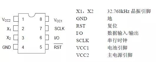
Figure 1 DS1302 Package Diagram
The internal structure of DS1302 is shown in Figure 2, the main components include:Shift register, control logic, oscillator, real-time clock, and RAM.Although the data is divided into two types, from the perspective of the microcontroller’s program, they are essentially the same, which is to perform read and write operations on specific addresses.
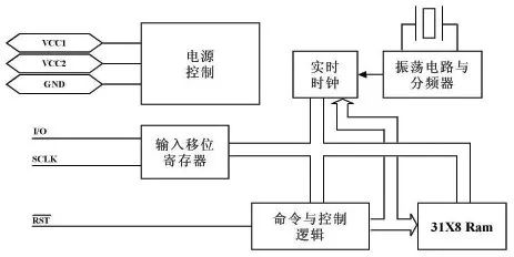
Figure 2 Internal Structure Diagram of DS1302
DS1302 contains a charging circuit that can charge the rechargeable battery used as a backup power source, and can choose the number of charging enable and series diodes to adjust the battery charging voltage.However, for us currently, the most important part to familiarize ourselves with is the clock-related functionality. For other parameters, please refer to the datasheet.
2. Working Principle of DS1302
To initialize any data transfer while working, DS1302 requires the reset pin (RST) to be set high and the 8-bit address and command information to be loaded into the shift register.Data is serially input on the rising edge of the clock (SCLK), the first 8 bits specify the access address, and after the command word is loaded into the shift register, during the subsequent clock cycles, data is output during read operations and output during write operations.The number of clock pulses in single-byte mode is 8+8 (8-bit address + 8-bit data), while in multi-byte mode it is 8 plus up to 248 data.
3. DS1302 Registers and Control Commands
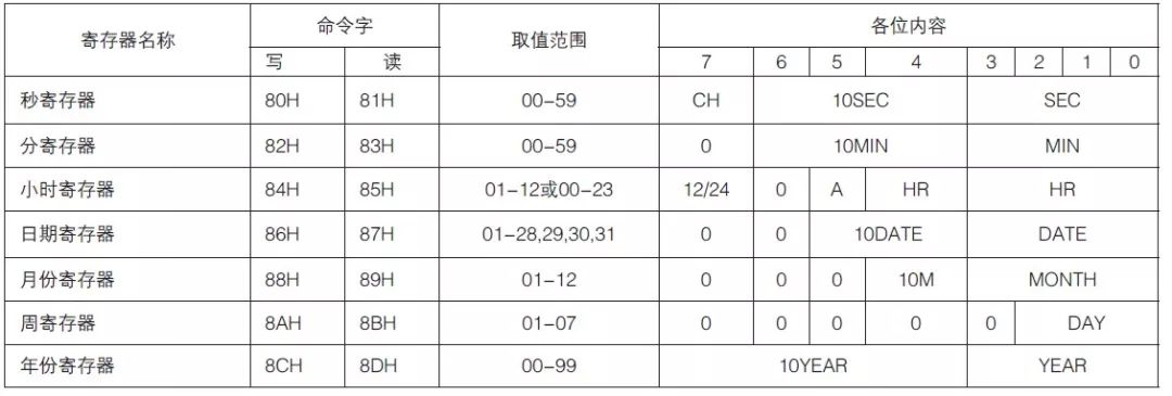
Operations on DS1302 are essentially operations on its internal registers. There are a total of 12 registers inside DS1302, of which 7 registers are related to the calendar and clock, storing data in BCD format.
In addition, DS1302 also has a year register, control register, charging register, clock burst register, and registers related to RAM.
The clock burst register allows for sequential read/write operations of all registers except the charging register.The calendar and time registers and control word are shown in Table 1.
Table 1 Calendar and Clock Register and Control Word Correspondence Table
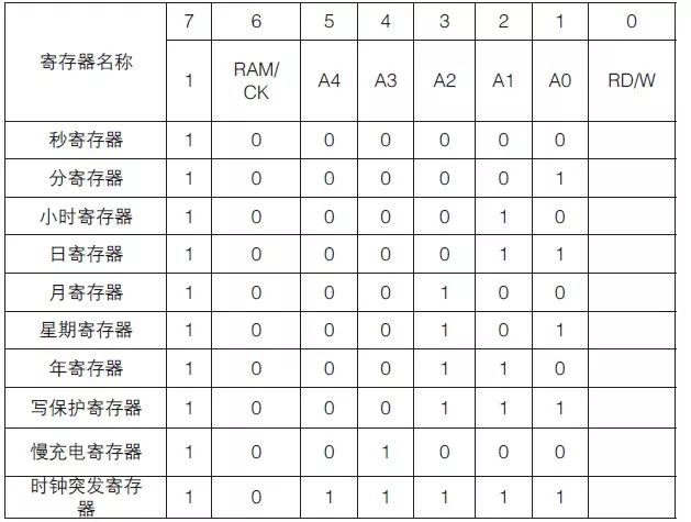
The last bit RD/W indicates “0” for write operations and “1” for read operations.
The internal register list of DS1302 is shown in Table 2.
The internal RAM of DS1302 is divided into two types, one type is a single RAM unit, with a total of 31 units, each unit being an 8-bit byte, with command control words from COH~FDH, where odd numbers are for read operations and even numbers are for write operations;the other type is RAM in burst mode, where all 31 bytes of RAM can be read/written at once, with command control words FEH (write), FFH (read).
Table 2 Distribution Table of Main Registers in DS14302
We now know the logical addresses of the control register and RAM, and next we need to know how to access these resources through the external interface.The microcontroller communicates with DS1302 via simple synchronous serial communication, and each communication must be initiated by the microcontroller. Whether it is a read or write operation, the microcontroller must first write a command frame to DS1302, with the highest bit BIT7 fixed at 1, BIT6 determining whether the operation is for RAM or clock registers, the next 5 bits are the internal address of RAM or clock registers in DS1302, and the last bit indicates whether this operation is a read or write operation.
Physically, the communication interface of DS1302 consists of 3 lines, namely RST, SCLK, and I/O.Where RST changes from low to high to start a data transmission process, SCLK is the clock line, and I/O is the data line.For specific read/write timing, refer to Figure 3, but please note that regardless of the synchronous communication type of the serial interface, it is sensitive to clock signals, and generally data writing is valid on the rising edge, while reading is valid on the falling edge (as is the case with DS1302, although not explicitly stated in the chip manual). If not particularly certain, the program design should be as follows:Keep SCLK low normally, set data before the clock changes, and read data after the clock changes, meaning that data operations are always performed while SCLK remains low, with an interval of one rising edge and one falling edge between adjacent operations.
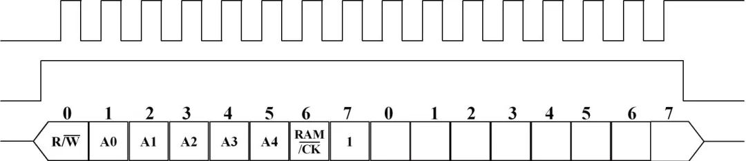
Figure 3 Command Word Structure of DS1302
Through the previous introduction of principles, we have a general understanding of the characteristics and working principles of the DS1302 clock chip. However, when we get a clock device, we may not know how to correctly apply it. For example, if we want to make a simple time display, what should we do?First, the connection between the clock chip and the microcontroller is very simple. Generally, we only need to connect the reset “RST”, data “I/O”, and clock “SCLK” terminals of the IIC device to the I/O ports of the microcontroller to write or read time and date data.Now, let’s look at an example of using DS1302 for time display. Through this example, I believe it will give everyone an intuitive understanding.
First, let’s take a look at the interface circuit of the DS1302 device on the enhanced PIC experiment board, as we need to consider how to program by combining software and hardware. The hardware schematic for completing this experiment is shown in Figure 4, where U2 is the DS1302 chip on the experiment board. The “I/O”
is connected to the microcontroller’s RB5 port, “SCLK” is connected to the microcontroller’s RB6, and “RST” is connected to the microcontroller’s RB7. The seven-segment displays D5, D7, and D8 form the display unit, and the character code data is fed into through the RC port, with the display chip select signals for each segment controlled by different RA ports.
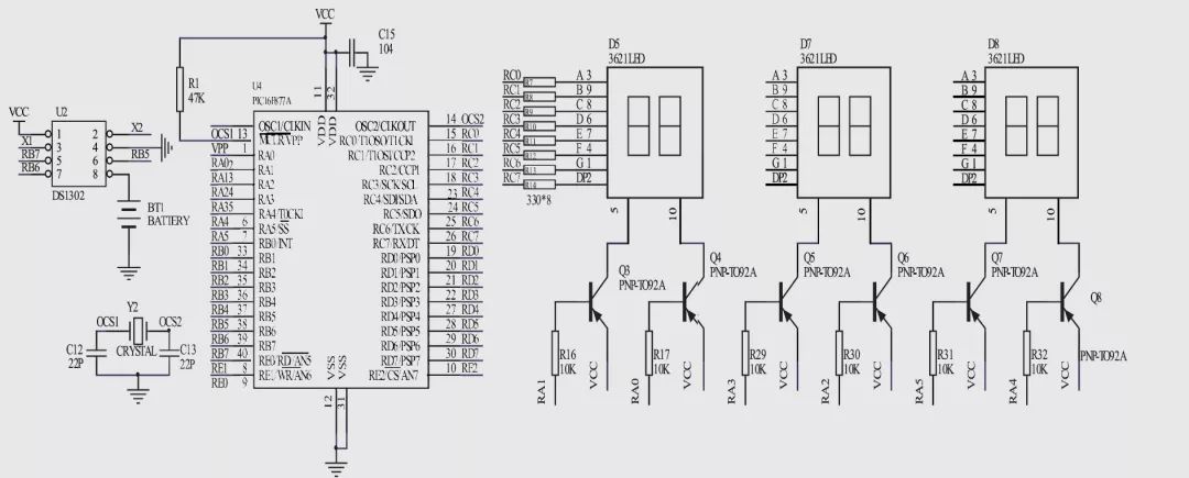
Figure 4 Hardware Schematic
For the programming of the standalone software, we use MPLab IDE software for C language programming, which serves as our programming environment. We can also perform program simulation debugging and burning steps by connecting the ICD2 emulator and enhanced PIC experiment board. The specific operational steps have been detailed in previous issues, so we will not repeat them here. Readers can refer to earlier articles or directly visit our website for more information.Now we can input the program code for debugging. We create a new project in MPLab IDE software, add the source code, and set the chip model and configuration bits. The chip model we are using for the experiment is PIC16F877A.The program code we wrote is as follows, with the program flowchart shown in Figure 5 and the actual running effect shown in Figure 6.
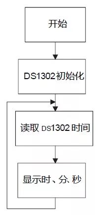
Figure 5 Software Flow
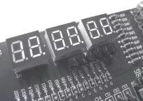
Figure 6 DS1302 Experiment Demonstration
2. Software Code
/*************************************************/
/*DS1302 Read/Write Demonstration Program */
/* Target Device:PIC16F877A */
/* Crystal Frequency:4.0MHZ */
/* Compile Environment:MPLAB V7.51 */
/**************************************************/
#include<pic.h>
#define i_o RB5
#define sclk RB6
#define rst RB7
unsigned char time_rx @ 0x30;
// Define reception register
static volatile bit time_rx7 @ (unsigned)&time_rx*8+7;
// Highest bit of reception register
/***************************************************/
Subfunction Definitions
**************************************************/
void port_init(); // Declare pin initialization function
void ds1302_init(); // Declare DS1302 initialization function
void set_time(); // Declare set time function
void get_time(); // Declare get time function
void display(); // Declare display function
void time_write_1(unsigned char time_tx);// Declare function to write one byte
unsigned char time_read_1();// Declare function to read one byte
void delay(); // Declare delay function
/***************************************************/
Time and Date Storage Table
**************************************************/
const char table[]={0x00,0x30,0x12,0x8,0x3,0x06,0x06,0x00};
char table1[7];
/**************************************************/
Common Cathode LED Segment Code Table
**************************************************/
const char table2[]={0xC0,0xF9,0xA4,0xB0,0x99,0x92,0x82,0xF8,0x80,0x90,0x88,0x83,0xC6,0xA1,0x86,0x8E};
void main()
{
port_init(); // Call pin initialization function
TRISC =0x00;
ds1302_init(); // Call DS1302 initialization function
set_time(); // Call set time function
while(1)
{
get_time(); // Call get time function
display(); // Call display function
}
}
void ds1302_init() // DS1302 initialization function subroutine
{
sclk=0; // Pull down clock signal
rst =0; // Reset DS1302
rst=1; // Enable DS1302
time_write_1(0x8e); // Send control command
time_write_1(0); // Allow writing to DS1302
rst=0; // Reset
}
void set_time() // Set time function subroutine
{
int i; // Define loop variable
rst=1; // Enable DS1302
time_write_1(0xbe); // Clock multi-byte write command
for(i=0;i<8;i++) // Continuously write 8 bytes of data
{
time_write_1(table[i]); // Call function to write one byte
delay();
}
rst=0; // Reset
}
void get_time() // Read time function subroutine
{
int i; // Set loop variable
rst=1; // Enable DS1302
time_write_1(0xbf); // Send multi-byte read command
for(i=0;i<7;i++) // Continuously read 7 bytes of data
{
table1[i]=time_read_1();
// Call function to read one byte of data
delay();
}
rst=0; // Reset DS1302
}
void time_write_1(unsigned char time_tx)
{
int j; // Set loop variable
for(j=0;j<8;j++) // Continuously write 8 bits
{
i_o=0; // Set data to 0 first
sclk=0; // Pull down clock signal
if(time_tx&0x01) // Check if the data bit to be sent is 0 or 1
{
i_o=1; // The data bit to be sent is 1
}
time_tx=time_tx》1; // Right shift the data to be sent by 1 bit
sclk=1; // Pull up clock signal
}
sclk=0; // After writing one byte, pull down the clock signal
}
unsigned char time_read_1()
{
int j; // Set loop variable
TRISB5=1; // Set data port direction to input
for(j=0;j<8;j++) // Continuously read 8 bits
{
sclk=0; // Pull down clock signal
time_rx=time_rx》1; // Right shift the reception register by 1 bit
time_rx7=i_o;
// Place the received data in the highest bit of the reception register sclk=1; // Pull up clock signal
}
TRISB5=0; // Restore data port direction to output
sclk=0; // Pull down clock signal
return(time_rx); // Return the read data
}
void port_init()
{
TRISA=0x00; // Set all A port to output
TRISC=0X00; // Set all C port to output
TRISB=0x00;
}
void display() // Display subroutine
{
int i; // Define lookup variable
i=table1[0]&0x0f; // Get the unit of seconds
PORTC=table2[i]; // Send to C port for display
PORTA=0xFD; // Light up the unit of seconds
delay(); // Delay for a while to ensure brightness
i=table1[0]&0xf0; // Get the tens of seconds
i=i》4; // Right shift by 4 bits
PORTC=table2[i]; // Send to C port for display
PORTA=0xFE; // Light up the tens of seconds
delay(); // Delay for a while to ensure brightness
i=table1[1]&0x0f; // Get the unit of minutes
PORTC=table2[i]&0x7f;
// Send to C port for display, and show decimal point
PORTA=0xF7; // Light up the unit of minutes
delay();
// Delay for a while to ensure brightness
i=table1[1]&0xf0; // Get the tens of minutes
i=i》4;
PORTC=table2[i]; // Send to C port for display
PORTA=0xFB; // Light up the tens of minutes
delay(); // Delay for a while to ensure brightness
i=table1[2]&0x0f; // Get the unit of hours
PORTC=table2[i]&0x7f;
// Send to C port for display, and add decimal point
PORTA=0xDF; // Light up the unit of hours
delay(); // Delay for a while to ensure brightness
i=table1[2]&0xf0; // Get the tens of hours
i=i》4;
PORTC=table2[i]; // Send to C port for display
PORTA=0xEF; // Light up the tens of hours
delay(); // Delay for a while to ensure brightness
}
void delay() // Delay program
{
int i; // Define integer variable
for(i=100;i–;); // Delay
}
At this point, I believe you can now complete some simple electronic clock experiments. We have covered the principles and usage of DS1302.
The enhanced PIC experiment board has rich system resources, and experiments can be conducted using:6-digit LED seven-segment displays, 8-channel LEDs, direct control keyboards, buzzer speakers, relay experiments, I2C bus interface, SPI bus interface, 160X LCD, 128X64 LCD, infrared receiver interfaces, stepper motor drive interfaces, AD conversion interfaces, serial clock chip DS1302, temperature sensor DS18B20 interfaces, RS232 serial communication, and external expansion interfaces for connecting more experimental resources.


To facilitate better learning for everyone, Changxue Electronics Network has specially added a public account for microcontrollers and EDA, pushing relevant knowledge daily, hoping to assist you in your studies!