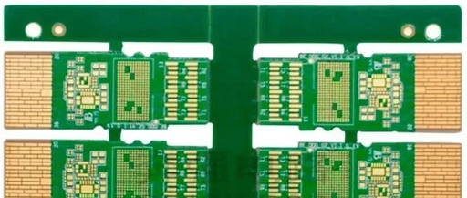
Avoiding Pitfalls in High-Speed PCB Design: 7 Key Aspects (Layer Stacking / Layout / Impedance Control Explained)

Avoiding Pitfalls in High-Speed PCB Design: 7 Key Aspects (Layer Stacking / Layout / Impedance Control Explained)

The biggest challenge in high-speed design is to minimize crosstalk, ensuring good signal integrity during transmission while also reducing the impact of noise on the PCB. Since single-ended signals and Low Voltage Differential Signaling (LVDS) are typical types of high-speed interface signals, it is essential to ensure the transmission of these two types of signals.In … Read more

Key Points of Signal Termination, Crosstalk, Filtering, and Decoupling Design in High-Speed PCB Design

Key Points of Signal Termination, Crosstalk, Filtering, and Decoupling Design in High-Speed PCB Design

[Image][Image] Long press to recognize and book online participation [Image] Long press to recognize and book offline gathering. The booking channel for offline and online appointments is about to close, so make an urgent reservation! ****************** The biggest challenge of high-speed design is to minimize crosstalk, ensure good signal integrity during transmission, and also reduce … Read more

How to Connect an Oscilloscope Probe?

How to Connect an Oscilloscope Probe?

If you do not have a probe, your oscilloscope will be incomplete, as the probe is an essential component that connects the device under test to the oscilloscope. The nature and quality of the probe will affect the accuracy of measurement displays and signal analysis. Probes are crucial for signal integrity, so you must choose … Read more

From Layer Stacking to Signal Integrity: Key Principles of PCB Multilayer Design for Beginners

From Layer Stacking to Signal Integrity: Key Principles of PCB Multilayer Design for Beginners

In the production of high multilayer PCBs, the drilling process directly determines the yield and reliability of the product. Industry data shows that the scrap rate of PCBs due to unreasonable hole diameter design can be as high as 30%, with poor hole processing in high multilayer boards accounting for over 45%. This article strictly … Read more

PCB Selection Guide: A Technical Manual Essential for Engineers

PCB Selection Guide: A Technical Manual Essential for Engineers

In the field of electronic design, the PCB selection guide is a core tool for engineers to avoid design risks and optimize product costs. A suitable circuit board, like a solid foundation, directly determines the performance, reliability, and market competitiveness of the final product. This guide aims to provide a systematic PCB selection framework to … Read more

Optimizing PORCH Parameters to Unlock LCD Screen Performance and Stability

Optimizing PORCH Parameters to Unlock LCD Screen Performance and Stability

In the hardware design of LCD screens and related LCD modules, precise configuration of timing parameters is fundamental to achieving optimal display performance and system stability. Among these, PORCH (blanking interval) settings are particularly critical—they define the exact boundaries of the pixel clock (PCLK), horizontal/vertical sync signals (Hsync/Vsync), front/back porches (HBP/HFP, VBP/VFP), and the active … Read more

Waveform Capture Rate: Definition, Principles, and Technical Implementation Explained

Waveform Capture Rate: Definition, Principles, and Technical Implementation Explained

Definition and Core Concepts of Waveform Capture Rate The Waveform Capture Rate is a key performance indicator of digital oscilloscopes, representing the number of times the oscilloscope can capture and display waveforms within a unit of time, typically measured in “captures per second” or “frames per second.” Its core significance lies in reflecting the oscilloscope’s … Read more

Novel Surface Finish for 5G-mmWave Frequency PCB Technologies: How to Achieve Optimum Signal Integrity

Novel Surface Finish for 5G-mmWave Frequency PCB Technologies: How to Achieve Optimum Signal Integrity

Editor’s Note: This article is excerpted from a presentation titled Novel Surface Finish for 5G-mmWave Frequency PCB Technologies: How to Achieve Optimum Signal Integrity. 0 Introduction With the increasing demand for high-frequency electronic devices, the shortcomings of traditional surface treatment processes such as electroless nickel immersion gold (ENIG) on printed circuit boards (PCBs) have become … Read more

Key Elements for Post-Design PCB Inspection!

Key Elements for Post-Design PCB Inspection!

When a PCB board has completed its layout and routing, and there are no errors reported in connectivity and spacing, does that mean the PCB is finished? The answer is certainly no. Many beginners, as well as some experienced engineers, often rush through the process due to time constraints, impatience, or overconfidence, neglecting the post-design … Read more

C-017: MIPI Interface PCB Layout and Routing Guide

C-017: MIPI Interface PCB Layout and Routing Guide

The MIPI (Mobile Industry Processor Interface) interface, especially its physical layers D-PHY and C-PHY, is widely used in high-speed data transmission scenarios such as cameras (CSI-2) and displays (DSI-2). The PCB layout and routing of MIPI are crucial for signal integrity, directly affecting the performance and reliability of devices. Below are key guidelines for MIPI … Read more