Remember when I first did PCB Layout, multi-layer board prototyping costs were very high, and the delivery time was about seven or eight days. Due to cost and time considerations, I often only considered using double-sided boards for routing. Then, holding many design rules that would often “conflict” with each other or experience-based rules circulating in BBS, I painfully struggled between signal lines and power/ground lines.
The result was that the current carrying capacity of the PCB routing was not adequately considered, and the power lines were routed like ordinary signal lines, causing the power lines to be too narrow, resulting in PCB temperature rise and voltage drop; at the same time, the layout of the ground line was also arranged last, prioritizing the signal lines; as a result, the ground line wandered back and forth between the top and bottom layers, creating many enormous return loops, which brought many inexplicable interferences to the signal lines, directly undermining confidence, and almost giving up before even starting.  .
Nowadays, with improved living standards, PCB manufacturing processes have also greatly improved. For example, now I log into Jialichuang to get a six-layer board, the cost and delivery time are beyond what I could have imagined when I just started working, and they also provide free prototyping services every month.
.
Nowadays, with improved living standards, PCB manufacturing processes have also greatly improved. For example, now I log into Jialichuang to get a six-layer board, the cost and delivery time are beyond what I could have imagined when I just started working, and they also provide free prototyping services every month.  With the innovation driven by Jialichuang, prototyping multi-layer boards has become very convenient, but to take full advantage of multi-layer boards, it’s not as simple as submitting the board files and waiting for the PCB factory to send the boards back to us. Although, relatively speaking, the more layers a PCB has, the easier it is to route, reasonable design requires additional considerations. Now, let’s start with the multi-layer board processes that PCB designers need to know.
1. The Development History and Trends of Multi-layer PCBs
Paul Eisler, an Austrian inventor, published a patent for printed circuit board manufacturing technology in 1936, which is closest to the current mainstream printed circuit board manufacturing form and is considered the origin of modern circuit boards. Therefore, Paul Eisler is also known as the father of PCBs.
With the innovation driven by Jialichuang, prototyping multi-layer boards has become very convenient, but to take full advantage of multi-layer boards, it’s not as simple as submitting the board files and waiting for the PCB factory to send the boards back to us. Although, relatively speaking, the more layers a PCB has, the easier it is to route, reasonable design requires additional considerations. Now, let’s start with the multi-layer board processes that PCB designers need to know.
1. The Development History and Trends of Multi-layer PCBs
Paul Eisler, an Austrian inventor, published a patent for printed circuit board manufacturing technology in 1936, which is closest to the current mainstream printed circuit board manufacturing form and is considered the origin of modern circuit boards. Therefore, Paul Eisler is also known as the father of PCBs.
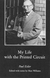
Paul Eisler, an Austrian inventor
Of course, even before this, as early as the early 20th century when the term “electronic devices” did not exist, people had the idea of manufacturing “circuit boards”. Since Alexander Graham Bell successfully demonstrated telephone communication in 1876, telephone communication began to develop rapidly; by 1904, there were 3 million telephone lines in the United States that needed manual telephone switching connections. This line-switching operation was labor-intensive. To solve the cumbersome problem of line-switching connections in the telephone system, the idea of manufacturing “circuit boards” appeared in patents as early as 1903.
The image shows the manual telephone exchange of the British company Huayang at No. 14 Hankou Road in 1907.
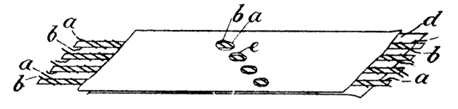
At that time, a famous German inventor named Albert Hanson applied for a patent. He pioneered the concept of using “lines” in telephone switching systems, using metal foil to cut into line conductors, then adhering wax paper between the line conductors, setting conductive holes at the intersections of the lines to achieve electrical interconnection between different layers. This is the early prototype of the “circuit board”.
Although the printed circuit board manufacturing technology was invented in 1936, due to the lack of supporting technologies related to PCB manufacturing at that time, such as the substrate for PCBs not being improved, and the vacuum tube being too large, heavy, and operating at high temperatures, PCB manufacturing technology was not widely applied in the production of electronic products until the 1950s.
Believed to be the “father of the plastic industry,” Belgian-American chemist Bakelite invented phenolic resin. Relying on Bakelite’s patents for the manufacture and application of phenolic resin, industrial production of phenolic resin was achieved, which also promoted the invention of phenolic paper laminates, which were first used in PCB manufacturing substrates in the 1940s in the United States.
After the invention of the transistor in 1947, transistors began to replace vacuum tubes in electronic products in the 1950s, and laminated phenolic paper substrates began to be widely used in the production of vacuum tube radios.
In 1947, epoxy resin began industrial production, and by the 1960s, commercial production of printed circuit boards had fully developed, and the mainstream PCB substrate began to shift to better-performing epoxy resin fiberglass substrates.
With the emergence of ICs (integrated circuits) and LSI (large-scale integrated circuits), electronic devices have developed towards a more compact, lightweight, short, and small direction, leading to a dramatic increase in routing density on PCBs, resulting in the transition of PCBs to multi-layer printed circuit boards.
By the 1980s, as circuit structures became increasingly complex, the number of layers in PCBs rapidly increased. At that time, almost all high-performance consumer electronic devices adopted multi-layer printed circuit boards, and the market demand for multi-layer PCBs expanded rapidly. Multi-layer substrate PCBs, as a fundamental emerging industry, rapidly expanded, and the most advanced PCB manufacturing technology at that time was already capable of producing multi-layer boards with up to 64 layers.
In the second half of the 1980s, the rapid development of the computer industry led to a significant increase in the production of multi-layer boards. At the same time, metal substrates such as aluminum-based substrates, ceramic multi-layer boards, and rigid-flexible combined boards also emerged.
In terms of interconnecting between routing layers, in addition to electroplating, there is also conductive paste via technology. Well-known technologies include Panasonic’s ALIVH and Toshiba’s B2IT (buried bump interconnection technology), which have propelled the application of circuit boards into the high-density interconnect (HDI) era.
2. Why Use Multi-layer PCB Structures for Design
With the increase in chip integration, the number of I/O pins in chip packaging has also increased dramatically, especially with the emergence of BGA packaging, relying solely on single-sided or double-sided conductor layer routing is no longer sufficient to route the pins in the inner circle of the BGA.
More importantly, with the rapid development of high-speed signal transmission, routing of high-speed signals requires the use of transmission line technology. In high-speed PCB design, it is essential to consider how to optimize the electrical interconnection performance of the routing while also controlling the manufacturing costs of the PCB. Factors affecting signal integrity, such as reflection, crosstalk, transmission delay, and switching noise (SSN), are major issues to be solved in high-speed circuit design.
There are several categories of transmission line technology. The earliest transmission line was the coaxial transmission line invented by Oliver Heaviside, used to solve the long-distance transmission problem of telegraphs at that time. Common forms of transmission lines on PCBs include microstrip and stripline.
Microstrip Transmission Line
Stripline Transmission Line
Stripline is a transverse electromagnetic (TEM) transmission line medium invented by Robert M. Barrett in the 1950s, while microstrip was developed two years later by ITT laboratories as a competitor to stripline.
Microstrip is located on the outer layer of the PCB, and since it is in contact with the external environment, it is easier for microstrip to radiate energy to the external environment, and it is also more susceptible to external environmental influences. For example, the change of the solder mask layer’s εr affects the characteristic impedance; therefore, the critical high-speed signals should prioritize using inner-layer routing, which is stripline transmission line.
Multi-layer boards also have dedicated complete power and ground layers, which not only increases the freedom of routing but also helps prevent signal interference and electromagnetic radiation, further promoting the development of multi-layer PCBs.
Now, with the improvement of IC processing technology, the rise time of digital signals has also been “passively” shortened. Previously, it was only necessary to consider routing through the PCB; more and more, it is necessary to consider transmission line effects during routing to better guide electromagnetic waves, avoid signal integrity issues, and meet EMC performance. Single-layer or double-layer boards find it challenging to provide sufficient space to construct a good transmission line structure given the current IC integration levels and routing densities. This necessitates the use of four-layer or even six-layer boards to transmit critical signals rich in higher harmonics using stripline.
With the development of semiconductor technology, we must consider using multi-layer boards to construct transmission lines for guiding electromagnetic waves. What should further popularize multi-layer boards is Jialichuang’s free prototyping activities.Currently, Jialichuang offers free prototyping services for 6-layer and 4-layer PCBs, allowing more partners to experience the ease of using multi-layer boards for routing, and now for 6-layer board prototyping, Jialichuang even provides free surface treatment of gold immersion process and via-in-pad process (resin plug + electroplating cap) as well.  For 6-layer boards, there will generally be BGA or QFN chips, and during SMT, there are requirements for the surface flatness of the PCB. Gold immersion pads have a flat surface, which is conducive to soldering, making it a perfect match for high-density multi-layer boards.
  Moreover, using Jialichuang’s via-in-pad process not only does not affect SMT soldering but also enhances product reliability and stability. The via-in-pad process can also save the surface routing space occupied by fan-out vias, further increasing the routing density on the surface. In addition, using the via-in-pad process allows the power/ground pads to connect directly to the main power/ground plane through vias, avoiding the influence of parasitic inductance from fan-out vias, which also helps with power integrity.
Jialichuang PCB Free Prototyping Rules
1. Use Jialichuang EDA design
No consumption amount is required, with no restrictions; you can receive 2 free prototyping coupons each month, supporting single (including aluminum-based), double, four, and six-layer boards.
2. Use other software for design
If the consumption amount exceeds 20 yuan, you can receive 2 free prototyping coupons in the next month, supporting single (including aluminum-based), double, four, and six-layer boards.
3. Scope of free prototyping coupon usage
Single, double, and four-layer free coupons: Length and width within 10CM, prototype 5 pieces, tin spraying, conventional process;
Six-layer free coupon: Length and width within 10CM, prototype 5 pieces, gold immersion, green, supports via-in-pad, conventional process;
Note: Six-layer boards need to be photographed after soldering, and must use BGA to pass the review.
3. The Manufacturing Process Flow of Multi-layer PCBs
There are two methods for manufacturing multi-layer boards: the electroplated via method and the high-density layer addition method, both of which achieve the circuit board structure through different process combinations. The electroplated via method is currently the most widely used, having undergone over half a century of development and improvement. It is quite mature in terms of equipment, materials, and processes, and has established a solid industrial foundation. The electroplated via method can produce both double-sided and multi-layer boards, and they can share the same processes and equipment. The electroplated via method is to penetrate the insulating substrate’s surface and internal conductor patterns with vias, electroplating a metal layer on the inner wall of the vias to connect the corresponding conductor patterns between different layers.
Here, I will take Jialichuang’s manufacturing process as an example. The typical main manufacturing process for rigid multi-layer boards is shown in the following flowchart:
The PCB factory does not directly manufacture copper-clad boards, prepregs, copper foils, etc., but purchases the required materials from upstream substrate manufacturers. The substrates are standard large sizes when they leave the factory, such as 1m x 1m (or 1m x 1.2m) specifications. Then, before PCB manufacturing, they need to be cut into sizes suitable for the production line according to their processing equipment specifications.
After cutting, for the multi-layer board process, the inner circuit is first made, such as inner layer pattern making, lamination, etc., and then the process returns to the same workflow as double-layer boards, such as drilling, electroplating, outer layer pattern making, etc. Finally, various inspections and packaging for shipment are done.
Inner Layer Pattern Making
The inner layers of multi-layer boards usually use thin double-sided copper-clad substrates. After forming the inner layer circuits on their surfaces, they are laminated to obtain multi-layer boards.
On the inner double-sided copper-clad board, a photosensitive dry film is attached, then a film with the inner layer circuit is attached and exposed. After exposure, development is performed, and then etching is done to remove unnecessary copper foil.
Once etching is complete, the inner layer circuits are revealed, and the protective film that protects the circuits from etching needs to be removed, which is the de-film process.
Next is the inspection of the inner layers, which is performed using Automatic Optical Inspection (AOI). Before lamination, to improve the bonding capability between the copper foil and the prepreg, a browning treatment is necessary.
The purposes of browning are as follows:
1) Increase the contact area between the copper foil and resin, enhancing the bonding force between the two;
2) Increase the wettability of the copper surface to the flowing resin, allowing the resin to flow into all corners and have stronger adhesion after curing;
3) Generate a fine passivation layer on the copper surface to prevent the hardener from reacting with copper under high temperature and pressure, which could generate water and cause board explosion.
The inner layer boards will be stacked according to the designed layering structure, stacking the prepared inner layer boards, prepregs, and outer copper foils in order, and then hot-pressed into one.
After lamination, the process for making outer layer circuits begins, which is consistent with the process for double-layer boards.
After the circuit board is laminated, the layers are not yet interconnected, so drilling is needed, followed by making conductive copper layers on the hole walls to achieve interconnection.
Chemical Copper Deposition and Overall Board Electroplating
Chemical copper deposition utilizes chemical methods to deposit a thin layer of copper on the insulating hole walls, while overall board electroplating increases the copper thickness on the already chemically deposited conductive walls. This mainly includes three processes: removing glue residue, chemical copper deposition, and copper electroplating.
Removing glue residue clears the glue residue from the holes and simultaneously creates micro-rough surfaces on the hole walls to enhance the bonding strength between copper and resin. Chemical copper deposition forms a thin metallic layer on the hole walls, serving as the seed layer for electroplating. Electroplating is to increase the copper thickness on the hole walls. Since there are no circuit patterns on the board surface at this time, this step is referred to as “overall board electroplating“. Jialichuang uses the industry’s cutting-edge pulse VCP, which has excellent penetration ability for small holes.
Outer Layer Circuit Patterns
The purpose is to transfer the outer layer circuits to the copper-clad board throughout the process.
The purpose of pattern electroplating is to electroplate a copper and tin layer to the required thickness on the exposed copper skin of the circuit pattern or on the hole walls.
The purpose is to remove the electroplating cover film using NaOH solution to expose the non-circuit copper layers.
The purpose of etching is to use chemical reaction methods to corrode the copper layers in non-circuit areas.
The main function of the circuit board is to carry and connect electronic components. After pattern electroplating, non-contact or soldering areas need to be protected with materials to safeguard these areas and prevent damage or oxidation. Components are usually soldered using solder paste, and these coated polymers are referred to as “solder mask”.
The purpose of characters is to provide an easy-to-recognize marking.
In the character process environment, I have marked it in parentheses () in the Jialichuang process flowchart above for distinction. The high-definition character process of Jialichuang is excellent, though the cost is relatively high, and everyone can choose according to their needs.
This differs from the “solder mask” process mentioned above, as it aims to protect the areas that need to be soldered or contacted, preventing bare copper foil from oxidizing due to exposure to air, which could cause poor soldering or contact issues.
The purpose is to punch or CNC mill the required shapes for customers using molds. Shaping methods include CNC milling, punching, manual milling, and hand cutting.
Note: CNC milling and punching have higher precision, followed by manual milling, and hand-cut boards are the lowest precision and can only make simple shapes.
Currently, Jialichuang has also added a “precision milling” process. The main difference between “regular milling” and “precision milling” lies in the positioning methods and processes. Regular milling uses external positioning, while “precision milling” uses internal positioning, with the regular milling process being a one-time milling, while the precision milling process involves two rounds of milling, one rough and one precise!
The purpose is to detect functional defects such as open circuits and short circuits that are not easily visible through electronic tests.
The purpose is to inspect product appearance defects and repair minor defects to prevent defective products from being released.
Jialichuang has recently upgraded their packaging for high-layer (6-20 layers) samples from punch boxes to more luxurious black and gold gift boxes, making them look more advanced and stylish.

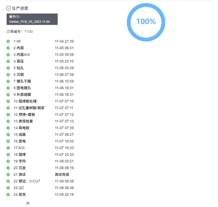
Additionally, they have developed an ordering assistant software that allows real-time tracking of the current production status of orders. Combined with the Jialichuang process flowchart above, one can be well-informed and comfortably wait for the arrival of the boards, which is a very good experience.


