Included in the collection
#Li Chengguang61
#Tape-Out1
The chip industry is no stranger to tape-out.
Tape-out refers to the process of manufacturing chips through a series of steps like an assembly line. This stage is a crucial link between chip design and mass production. In simple terms, it means handing over the designed scheme to the chip manufacturer to produce a few samples for testing to see if the designed chip works, followed by optimization. If the tests pass, mass production begins. Therefore, tape-out is essential for testing whether the integrated circuit design is successful, which is also a significant reason why chip design companies need to invest heavily in the early stages. The tape-out process is a critical step in getting a chip from design to mass production. Once the chip is fully designed, it needs to be etched onto the wafer according to the blueprint. The process technology used, the size of the wafer, and the complexity of the chip all affect the success rate and cost of tape-out. Moreover, many chips do not succeed in tape-out on the first try; often, multiple tape-outs are required to achieve satisfactory results.
 Image Source: Knowledge Vector
However, tape-out is an expensive endeavor. A few failed tape-outs can potentially bankrupt a company. In 2019, there were reports of Xiaomi’s Pinecone Electronics’ Pangu S2 series chips failing tape-out five times in a row, leading to a painful restructuring of the design team. A major chip manufacturer calculated that for a 14nm process chip, one tape-out costs about $3 million; for a 7nm process chip, it costs around $30 million; and for a 5nm process chip, it can reach $47.25 million. Clearly, tape-out represents a significant expenditure for chip design companies, especially for small and medium-sized enterprises in the industry, where the actual tape-out price is much higher than that of larger firms, exacerbating their already limited financial resources.
Why Is Tape-Out So Expensive?
So, why is the cost of chip tape-out so high?
This brings us to the principles of chip manufacturing. Chip manufacturing involves placing billions of transistors on a very small chip, and the manufacturing process has reached the nanometer level, which can only be accomplished using lithography. Lithography is the process of creating desired patterns using light, requiring the use of masks (also known as photomasks). The mask is where the designed circuit diagram is engraved, allowing light to pass through and etch the pattern onto the wafer. The high cost of tape-out is partly due to the need to verify many processes initially; from a circuit diagram to a chip, every step must be validated to ensure the circuit meets the required performance and functionality. The tape-out process lasts at least three months (including material preparation, lithography, doping, plating, packaging, and testing), generally involving over 1,000 process steps, making it the most critical and costly stage in chip manufacturing. If tape-out is successful, large-scale chip production can commence; otherwise, the reasons must be identified, and corresponding optimizations must be made. The primary costs associated with tape-out arise from the mask and the wafer, both of which are expensive consumables, with the mask being the most costly. A set of mid-range process masks costs about $500,000, while a single wafer can cost several thousand dollars.
Which Is More Expensive: The Mask or the Wafer?
The mask is made of quartz and serves as a graphic transfer tool or template in the microelectronics manufacturing process, functioning similarly to the “film” of a traditional camera. Based on the required graphics, fine patterns at the micron and nanometer levels are etched onto the mask substrate using lithography. The process of transferring the mask’s graphics onto the wafer can be likened to the workflow of a banknote printing machine. The lithography machine is akin to the printing press, the wafer is like the printing paper, and the mask is the printing plate, where the graphic of the banknote template is printed onto the paper, just as the lithography machine prints the chip graphics from the mask onto the wafer. Lithography requires the use of masks, which engrave the designed circuit diagram, allowing light to pass through and etch the pattern onto the wafer.
 Principle of Lithography
The quality of the mask directly affects the quality of lithography. Manufacturing defects and errors on the mask will be introduced into the chip manufacturing process along with the lithography process. Therefore, the mask is one of the determinants of precision and quality for downstream products. The price of the mask primarily depends on the “process node” chosen for the chip; the higher the process node, the more expensive the tape-out. This is because more advanced process nodes require more layers of masks. Reports indicate that approximately 60 masks are needed for 14nm processes, while 7nm may require 80 or even over 100 masks. More layers of masks not only increase the cost of the masks but also necessitate additional lithography steps, reapplying photoresist, further exposure, and additional development… The overall cost increases significantly. According to IBS data, the mask cost for 16/14nm processes is around $5 million, while for 7nm processes, the mask cost quickly rises to $15 million.
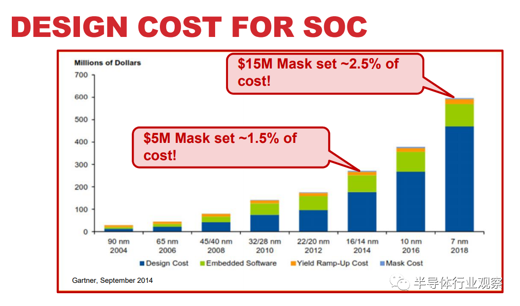 The mask cost in 7nm processes is approximately $15 million
(Image Source: IBS)
The overall cost of the mask includes the cost of raw materials such as quartz and photoresist, as well as the usage costs of Mask Writers and Inspection equipment. Additionally, there are costs associated with generating mask-related data, including software licenses and server usage for OPC, MDP, and other processes. For a single chip, masks can involve dozens of layers, requiring a multitude of steps, equipment, software, and personnel, which naturally results in high costs. In the tape-out process, the cost of the mask is a significant portion, as the early tape-out phase involves producing 5-25 chips for product validation, with the primary cost being the mask. In contrast, during formal production, the mask cost is counted only once, and the subsequent large quantity of wafers can share the cost, making it cheaper. More accurately, the cost averaged per chip becomes cheaper, rather than the total tape-out cost decreasing. Industry insiders reveal that a foundry’s tape-out cost at 40nm is approximately $600,000 to $900,000, with the mask accounting for a significant portion, around $600,000 to $900,000; the wafer cost is around $3,000 to $4,000 each. Therefore, if producing 10 wafers, the cost per wafer is ($900,000 + $4,000 * 10) / 10 = $94,000; however, if producing 10,000 wafers, the cost per wafer becomes ($900,000 + $4,000 * 10,000) / 10,000 = $4,090. It is evident that once mass production begins, producing tens of thousands of wafers can reduce the cost per wafer to around $3,000 to $4,000, significantly lowering the mask cost per wafer. Thus, during the small-volume tape-out phase, the mask cost is the main expense. Conversely, during high-volume production, the wafer becomes the primary cost driver. Additionally, semiconductor manufacturing equipment can cost hundreds of thousands to over a billion dollars. For instance, the mask equipment for 28nm exceeds $50 million per unit, and such machinery typically depreciates over seven years. This means that approximately 14% of the machine’s value is lost each year. The depreciation period for foundry equipment is usually 5-7 years. Reports indicate that SMIC’s depreciation costs exceeded 1.4 billion in 2019, primarily due to the need to purchase high-priced machinery for advanced processes, resulting in increasing depreciation costs each year. TSMC’s depreciation costs reached nearly 100 billion New Taiwan dollars in 2021, setting a record high. From the perspective of process development cycles, the costs and depreciation of machines are already substantial, but achieving yield and reliability standards for mass production is also a challenging task. (It is reported that a certain factory’s 28nm machines arrived in 2011/2012, but even after 5 or 6 years, the yield had not met strict mass production standards, highlighting the difficulty. Meanwhile, they also incurred years of unnecessary depreciation costs.) Additionally, there are labor costs, maintenance costs, and consumable expenses, all contributing to the high mask costs. According to etnews, due to the current supply-demand imbalance, mask prices are rising, and delivery times are being extended. Even with extra payments, it is challenging to purchase masks promptly. The typical delivery time of 4-7 days has recently increased to 14 days, and some companies have seen delivery times extend to seven times their original duration. Furthermore, to keep pace with Moore’s Law, foundries’ investments in upgrading equipment and technology development are continually increasing, ultimately passing these costs onto customers’ tape-out fees. This has led to a continuous rise in chip manufacturing costs.
How to Reduce Tape-Out Costs?
Under these various influences, the cost of chip tape-out has become a significant challenge for design companies.So, in the face of high tape-out prices, is there any way to reduce costs?
Wang Long, a senior director at Moore Elite, indicated that MPW (Multi-Project Wafer) is a tape-out method that can help design companies reduce costs.MPW refers to a wafer shared by multiple projects, where a single manufacturing process can accommodate the manufacturing tasks of multiple IC designs. Several integrated circuit designs using the same process are placed on the same wafer for tape-out, and after manufacturing, each design can obtain dozens of chip samples, which is sufficient for experimental and testing purposes during the prototype design phase. Simply put, several companies or institutions jointly purchase a set of masks, and the same wafer produced will contain several different chips, which can be “picked up” by each party after the wafer is cut. The manufacturing costs are then shared among all participating MPW projects based on chip area, significantly reducing product development risks. According to Wang Long, MPW has a specific process, typically organized by foundries or third-party service agencies. The scheduling of various processes for MPW throughout the year is pre-established, with more advanced processes having higher MPW frequencies. Foundries will pre-divide the wafer into multiple regions and quote prices, allowing companies to reserve one or more regions based on their needs. This imposes certain time pressures on participants regarding design and development. However, the benefits of MPW are evident; using multi-project wafers can lower chip production costs, provide practical opportunities for designers, and facilitate the transformation of chip design results, significantly aiding the training of IC design talent, the development of small and medium-sized design companies, and the research and development of new products. In comparison, the benefit of shared masks is cost-saving, but it may require waiting for the foundry’s scheduling, thus taking more time. For companies that are not financially constrained or are in a hurry, they can utilize a full-mask (Full-Mask), where all masks in the manufacturing process are dedicated to their designs, typically used in the mass production phase after design finalization. Once the machines are running, the profits can be substantial. However, in the current context of severe capacity shortages, foundries respond differently to customer product demands, competitive advantages, market prospects, and plans. They will comprehensively consider order volumes, order stability, and market prospects when making judgments. In reality, for most small and medium-sized enterprises, aside from price, they also face numerous challenges in the tape-out or mass production stages, including capacity and delivery times:
1. Lack of understanding of the foundry system and experience in process selection and communication with foundries;
2. High entry barriers for mainstream foundries, making it difficult for emerging players to apply for expected processes or support, leading to high communication costs;
3. Lack of systematic supply chain management capabilities, especially during the ramp-up phase of mass production, being overly optimistic about capacity, delivery times, and quality;
4. In a tight capacity situation, lacking a stocking mechanism, panic ordering or placing orders only after receiving orders leads to capacity not keeping up with market demand. Additionally, fluctuations in delivery times and capacity significantly increase communication costs between startup companies and foundries, reducing efficiency.
In response,small and medium-sized chip design companies can seek collaboration with third-party operational service organizations that have resources, strength, and experience to address supply chain challenges.
For example, Moore Elite’s tape-out services provide a complete process platform, connecting dozens of mainstream foundries and offering tape-out services across different process nodes, including MPW, full-mask, and mass production, significantly reducing customers’ business costs and communication costs.On the other hand, with its in-house professional tape-out FAE team, it not only provides efficient support management for foundries’ long-tail customers but also helps small and medium-sized companies’ products receive support quickly, assisting customers in selecting optimal processes and ensuring data security. Regarding capacity, Moore Elite leverages its know-how to help small customers secure capacity (including large orders, order trends, early queuing, and timely tracking of capacity dynamics), helping customers reduce costs and shorten chip development cycles. Overall, whether from a technical, business, or capacity perspective, choosing a reliable third-party organization can assist design companies in addressing current supply chain challenges and providing optimal solutions. In summary, companies in these demand tracks may benefit from the services of tape-out vendors.
Final Thoughts
A chip development project requires a lengthy process from product definition, design, validation, and simulation to final tape-out. As the “ultimate exam,” any small oversight during this lengthy process can lead to tape-out failure, which often means a company faces losses starting from tens of millions of dollars and a missed market opportunity of at least six months. For many companies, tape-out failure is an unbearable pain. In this regard, chip design companies, manufacturers, and related industry service platforms and organizations should closely collaborate, complementing each other’s strengths to jointly address the “tape-out dilemma” that developers face.
*Disclaimer: This article is original by the author. The content reflects the author’s personal views, and Semiconductor Industry Observation reproduces it only to convey a different perspective, which does not represent its endorsement or support of the viewpoint. If there are any objections, please contact Semiconductor Industry Observation.