

In the current era where the scale of artificial intelligence models is growing exponentially to trillions of parameters, traditional chip architectures are facing unprecedented performance and energy efficiency bottlenecks. While an NVIDIA H100 GPU cluster takes several weeks to train the Llama70B model, the wafer-scale computing platform Cerebras WSE-3 can complete the same task in just one day. This technological revolution, triggered by physical limits, has begun. Wafer-Scale AI Computing integrates millions of computing cores and massive on-chip storage on a single silicon wafer, achieving ultra-low latency data flow within the chip and reducing inter-chip communication costs to negligible levels. However, breakthroughs at the hardware level are just the starting point of this transformation; the key to its success lies in the reconstruction of system software—this is the historical mission undertaken by the WaferLLM system jointly developed by Microsoft Research Asia and the University of Edinburgh.
1. Performance Traps of Traditional Architectures and Breakthroughs in Wafer-Scale Computing
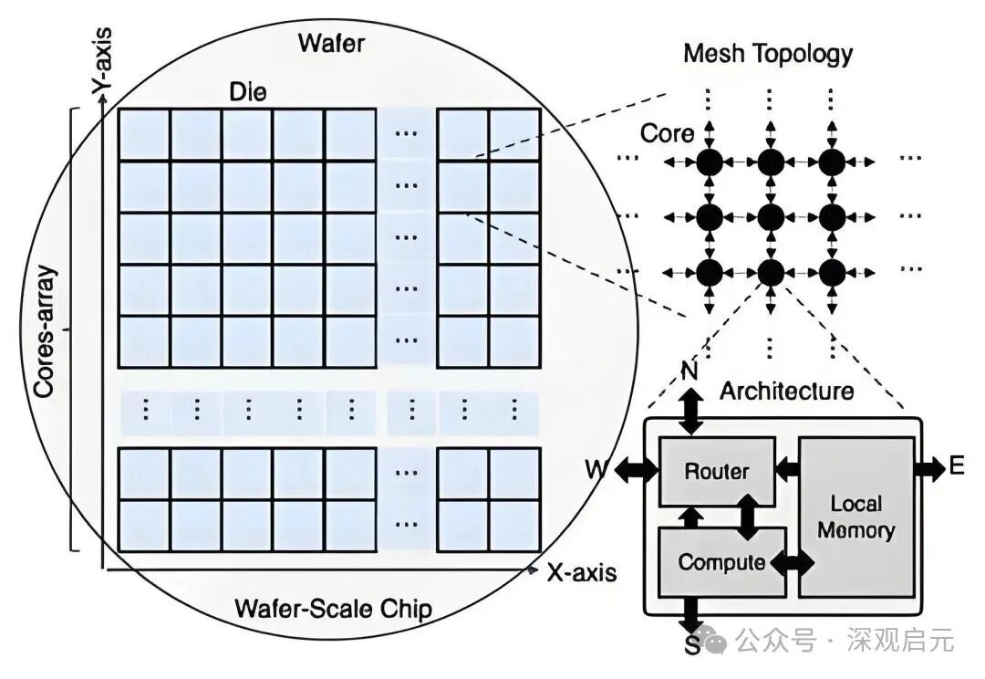
Traditional chips are limited by a photolithography exposure window of 26mm×33mm, constraining the area of a single chip to within 858mm². When AI model parameters exceed the trillion level, the computational power gap caused by this area constraint expands exponentially. The NVIDIA H100, with a 7nm process, achieves a chip area of 542mm² and integrates 81,920 CUDA cores, yet even so, its single-chip computational power still cannot meet the demands of large model training. In contrast, the Cerebras WSE-3, through wafer-scale integration technology, integrates 40 trillion transistors, 900,000 AI cores, and 44GB of on-chip SRAM on a 46,225mm² wafer, creating a peak computational power of 125PFlops. This breakthrough is not only due to the increase in physical size but also due to the construction of 21PB/s on-chip memory bandwidth through wafer-scale redistribution layers (RDLs) and local silicon interconnect (LSI) technology—7000 times that of traditional GPU clusters.However, the leap in hardware does not automatically translate into system-level advantages. When researchers attempted to form a cluster with 8 A100 GPUs, the decoding rate only increased from 78 tokens/s to 260 tokens/s, far from the theoretical 8-fold expansion. This “scaling efficiency decay” exposes the fatal flaws of traditional system software: the MPI architecture based on distributed memory models, thread scheduling mechanisms optimized for small core counts, and a lack of understanding of wafer-scale interconnect topologies collectively form the shackles that restrict performance release.
2. System Reconstruction: Full-Stack Innovation from Compiler to Runtime
The WaferLLM system proposed by Microsoft Research Asia achieves deep adaptation to wafer-scale hardware characteristics through three innovations. First, at the compiler level, its developed Wafer Native Compiler introduces dynamic topology-aware technology, which can automatically generate optimal inter-core communication paths based on the 2D mesh interconnect structure of wafer-scale chips. This graph neural network-based compilation strategy elevates traditional compiler static optimization to a new dimension of dynamic topology awareness, reducing communication overhead by 42%.Secondly, the reconstruction of the runtime system overturns traditional task scheduling paradigms. In tests with the Cerebras WSE-2, WaferLLM compresses the processing latency of each token to sub-millisecond levels through fine-grained task slicing and asynchronous pipelining techniques. Compared to vLLM on 8 A100 GPUs, the wafer-scale platform increases the decoding rate to 2700 tokens/s while maintaining the same energy efficiency ratio (0.92) and reducing inter-node communication costs to zero. This breakthrough is attributed to the runtime system’s deep utilization of the wafer-scale memory hierarchy—by directly mapping KV caches to on-chip storage, it avoids the frequent cross-chip data transfers common in traditional clusters.Most revolutionary is the innovation of the programming model. The traditional MPI model reveals significant limitations under wafer-scale architectures: its process-based abstraction struggles to adapt to million-core level parallelism and lacks awareness of wafer-scale interconnect topologies. The Wafer-Native Programming Model proposed by WaferLLM introduces distributed shared memory (DSM) abstraction and topology-aware task schedulers, allowing developers to manage wafer-scale resources as if they were operating a single chip. This paradigm shift reduces the inference latency of the Llama70B model from 3.2 seconds on GPU clusters to 0.35 seconds while improving the energy efficiency ratio to 2.22.3. The Leap from Laboratory to Industrialization
In actual tests with the Cerebras WSE-2, WaferLLM demonstrated astonishing scalability. As model parameters scaled from tens of billions to trillions, the performance improvement of traditional GPU clusters gradually slowed, while the acceleration ratio of the wafer-scale platform continued to grow. In the test-time scaling test with 128B parameters, the throughput of the wafer-scale system reached 17 times that of GPU clusters while reducing energy consumption to one-fifth. This performance leap is not only due to breakthroughs at the hardware level but also benefits from the deep adaptation of system software to wafer-scale architecture—by dynamically adjusting the activation modes of computing cores, WaferLLM can automatically optimize resource allocation under different workloads.However, the popularization of wafer-scale computing still faces multiple challenges. Thermal management issues become more complex as wafer sizes increase, and the liquid cooling framework used by Tesla’s Dojo system needs to deeply match the thermal requirements of wafer-scale chips. In terms of software ecology, mainstream deep learning frameworks (such as PyTorch and TensorFlow) still lack native support for wafer-scale architectures, necessitating the development of new distributed training algorithms and automatic parallelization tools. Additionally, the manufacturing yield of wafer-scale chips—Cerebras’ yield typically ranges from 20% to 30%—also places higher demands on system software: designing fault tolerance mechanisms to maintain system stability in the event of partial core failures becomes an urgent technical challenge.4. Future Outlook: From Computational Power Revolution to Reconstruction of Intelligent Forms
Wafer-scale computing is redefining the boundary conditions of AI systems. While traditional chips are constrained by the “area-power-performance” triangle dilemma, wafer-scale architectures break this shackles through system-level reconstruction. Predictions from Microsoft Research indicate that by 2027, AI clusters built with wafer-scale chips will achieve a computational power density of 1EFlops per rack, 200 times that of current GPU clusters. This leap in computational power will not only push large model training into the “hour-level” era but also give rise to entirely new intelligent forms—from localized large model deployment on edge computing devices to the realization of quantum-classical hybrid computing architectures, wafer-scale platforms are opening new doors to general artificial intelligence (AGI).In this technological revolution, the reconstruction of system software plays a crucial role. As revealed by Academician Wu Jiangxing’s team with the “Software Defined System on Chip Technology” (SDSoW), by deeply integrating software-defined architecture with wafer-scale integration, system performance is expected to achieve a 3 to 5 orders of magnitude improvement. When hardware innovation and software reconstruction resonate, the boundaries of AI computational power will no longer be limited by the physical limits of silicon-based materials but will depend on the co-evolution capabilities of systems and intelligence. This may be the ultimate revelation brought by wafer-scale computing: in the next stage of the computational power revolution, the real breakthroughs will come from the paradigm shifts triggered by collaborative innovation between hardware and software.





X Media Officer | Kevin 138 8041 8738