UART, I2C, and SPI are the three most commonly used communication protocols in microcontroller systems. In this lesson, we will learn about the remaining SPI communication protocol.
SPI stands for Serial Peripheral Interface. As the name suggests, it is a serial interface for peripheral devices. SPI is a high-speed, full-duplex, synchronous communication bus that typically uses only 4 pins. It is commonly used for communication between microcontrollers and devices such as EEPROM, FLASH, real-time clocks, and digital signal processors. The communication principle of SPI is simpler than that of I2C; it primarily operates in a master-slave mode, usually with one master and one or more slaves. The standard SPI uses 4 lines: SSEL (Slave Select, also written as SCS), SCLK (Clock, also written as SCK), MOSI (Master Output/Slave Input), and MISO (Master Input/Slave Output).
SSEL: The slave device select enable signal. If the slave device is enabled by a low level, pulling this pin low will select the slave device, allowing communication between the master and the selected slave.
SCLK: The clock signal generated by the master, which is somewhat similar to the SCL in I2C communication.
MOSI: The channel through which the master sends commands or data to the slave.
MISO: The channel through which the master reads the status or data from the slave.
In some cases, we can also communicate using a 3-wire or 2-wire SPI. For example, when the master only sends commands to the slave and does not need to receive data, MISO can be omitted; conversely, when the master only reads data from the slave and does not need to send commands, MOSI can be omitted. When there is one master and one slave, the slave’s select signal can sometimes be fixed at a valid level, keeping it enabled, allowing SSEL to be omitted. If the master only sends data to the slave, both SSEL and MISO can be omitted; if the master only reads data from the slave, both SSEL and MOSI can be omitted.
It is important to understand the 3-wire and 2-wire SPI, as they have practical applications. However, when we refer to SPI, we generally mean the standard SPI, which involves the use of 4 lines.
The master of SPI communication is also our microcontroller. During the process of reading and writing data, there are four modes. To understand these four modes, we must first learn about the following two terms.
CPOL: Clock Polarity. What does clock polarity mean? The entire communication process can be divided into idle and communication states. If SCLK is high during the idle state before and after data transmission, then CPOL=1; if SCLK is low during the idle state, then CPOL=0.
CPHA: Clock Phase.
When the master and slave exchange data, it involves the timing of when the master outputs data to MOSI and when the slave samples this data, or when the slave outputs data to MISO and when the master samples this data. A characteristic of synchronous communication is that all data changes and sampling occur with clock edges, meaning data changes or is sampled around the clock edges. A clock cycle must include both a rising edge and a falling edge, as defined by the cycle, but the order of these edges is not specified. Additionally, since data requires a certain amount of time to stabilize after being generated, if the master outputs data to MOSI on the rising edge, the slave can only sample this data on the falling edge. Conversely, if one party outputs data on the falling edge, the other party must sample it on the rising edge.
CPHA=1 means that data output occurs on the first edge of a clock cycle, and which edge it is (rising or falling) depends on the value of CPOL. If CPOL=1, it is the falling edge; if CPOL=0, it is the rising edge. Thus, data sampling naturally occurs on the second edge.
CPHA=0 means that data sampling occurs on the first edge of a clock cycle, and which edge it is is determined by CPOL. Therefore, data output occurs on the second edge. Consider this: when the first bit of a data frame begins transmission, if it is sampled on the first clock edge, when is it output? There are two scenarios: one is at the edge when SSEL is enabled, and the other is at the last clock edge of the previous data frame, and sometimes both conditions may be effective simultaneously.
Taking CPOL=1/CPHA=1 as an example, we illustrate the timing diagram as shown in Figure 15-1.
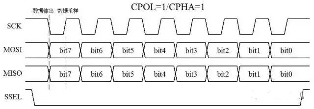
Figure 15-1 SPI Communication Timing Diagram (1)
As shown in Figure 15-1, when no data is being sent and after transmission is complete, SCK is high, thus CPOL=1. It can be seen that at the first edge of SCK, MOSI and MISO change, while at the second edge of SCK, the data is stable, making it the appropriate moment to sample data. This means that the rising edge captures the data at the end of one clock cycle, thus CPHA=1. Note the often overlooked SSEL signal, which is typically used to determine which slave device is communicating with the master. The remaining three modes can be illustrated in a simplified timing diagram where MOSI and MISO are combined for clarity. Please carefully compare and study these diagrams to thoroughly understand the theoretical process, which will help deepen your understanding of SPI communication, as shown in Figure 15-2.
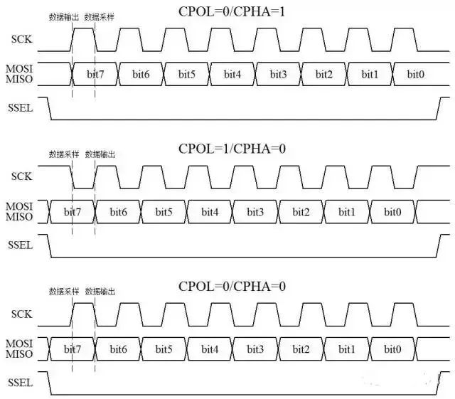
Figure 15-2 SPI Communication Timing Diagram (2)
In terms of timing, isn’t SPI much simpler than I2C? There are no start, stop, or acknowledgment signals. UART and SPI only handle communication without caring about whether the communication was successful, while I2C relies on acknowledgment information to determine the success or failure of communication. Therefore, comparatively speaking, the timing of UART and SPI is simpler than that of I2C.