#
Click the blue text to follow us and never miss exciting content
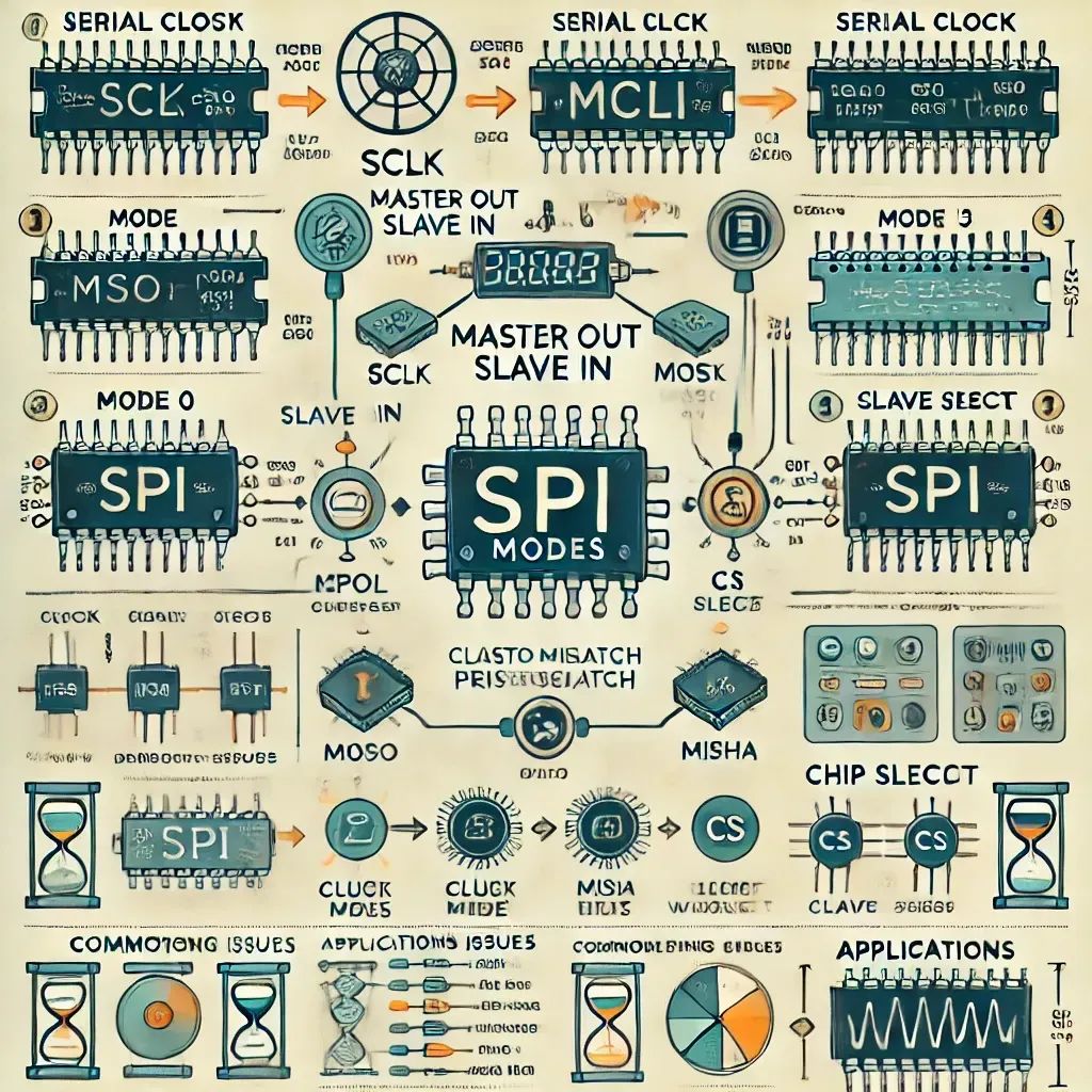
Origin of SPI
The SPI interface was first proposed by Motorola (now NXP) for high-speed data transfer between processors and peripheral devices. Due to its simplicity, efficiency, and low resource consumption, it quickly gained widespread adoption and became one of the most common communication protocols in embedded systems.
Signal Transmission Mode of SPI
SPI adopts a master-slave architecture, typically consisting of one master controlling one or more slaves. The communication method is based on full-duplex data transmission and mainly includes the following signal lines:
- • SCLK (Serial Clock): The clock signal provided by the master, controlling the data transfer rate.
- • MOSI (Master Out Slave In): The signal line for the master to send data to the slave.
- • MISO (Master In Slave Out): The signal line for the slave to send data to the master.
- • CS/SS (Chip Select/Slave Select): Active low enables the slave to identify whether it is communicating with the master.
The three-wire SPI mode typically omits CS/SS, keeping it enabled in the circuit.
Four Modes of SPI (Clock Polarity and Phase)
SPI communication is determined by CPOL (Clock Polarity) and CPHA (Clock Phase), resulting in four modes:
| Mode | CPOL | CPHA | Idle Clock State | Sampling Time |
| Mode 0 | 0 | 0 | Low Level | Sample on Falling Edge |
| Mode 1 | 0 | 1 | Low Level | Sample on Rising Edge |
| Mode 2 | 1 | 0 | High Level | Sample on Rising Edge |
| Mode 3 | 1 | 1 | High Level | Sample on Falling Edge |
Different SPI devices may use different modes, and the SPI modes of the master and slave must match during use.
Electrical Parameters of SPI
The electrical characteristics of SPI vary by device, focusing primarily on the following parameters:
- • Operating Voltage (Vcc): Typically 3.3V or 5V.
- • Clock Frequency (SCLK): Depends on the capabilities of the master and slave, typically ranging from a few hundred kHz to tens of MHz.
- • Logic Levels: Typically conform to CMOS/TTL standards, with high and low level thresholds matching the system power supply voltage.
- • Pull-up/Pull-down Resistors: The chip select (CS) pin typically requires a pull-up to maintain a high level when not selected.
Application Design of SPI
Typical Application Scenarios
- • Sensor Interface: Such as accelerometers (MPU6050), temperature and humidity sensors, etc.
- • Storage Devices: Such as Flash (W25QXX series), EEPROM (AT25 series).
- • Displays: Such as OLED, LCD (ST7789, ILI9341).
- • Communication Modules: Such as WiFi, LoRa, RFID, and other wireless communication modules.
Common Issues and Solutions
| Issue | Possible Cause | Solution |
| No Communication | Clock polarity/phase mismatch | Ensure consistency in master-slave mode |
| Data Transmission Error | Signal integrity issues, clock rate too high | Reduce SCLK frequency, check signal quality |
| Chip Select Abnormality | Chip select signal interference or not properly pulled high/low | Properly add pull-up resistors |
| Confusion in Multi-Slave Communication | CS signal conflict | Ensure only one slave CS is active |
| Data Misalignment | Clock and data sampling timing mismatch | Calibrate CPOL and CPHA settings |
Disclaimer:
This account maintains neutrality regarding all original and reprinted articles’ statements and viewpoints, and the articles are provided solely for readers’ learning and communication. Copyrights for the articles, images, etc., belong to the original authors. If there is any infringement, please contact us for deletion.