EETOP focuses on chips and microelectronics. Click on the blue text above to follow us.

Nowadays, portable devices have become increasingly prevalent in people’s daily lives. Mobile phones, iPads, and computers have become necessities, even my grandmother has started using a smartphone for video calls and browsing Douyin. Besides performance and size, battery life is the most concerning issue for portable devices. A few years ago, a certain mobile phone manufacturer even advertised “5 minutes of charging for 2 hours of talk time.”
Excessive power consumption generates more heat, and overheating can affect device performance, causing smartphones and computers to lag. We must also consider how to dissipate heat and increase cooling components, which further adds to cooling costs.
-
Basic Concepts in Low-Power Design
Dynamic power and Leakage power:
In the process of digital IC design, power mainly refers to dynamic power consumption and leakage power consumption.
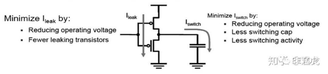
In digital circuits, if there is a signal flip, then dynamic power consumption exists, while leakage power consumption is always present.
Generally, dynamic power consumption is much greater than static power consumption, but since static power consumption is always present, we cannot ignore it.
2. General Methods for Low-Power Design:
a. Clock-based low-power design
The design idea of this method is to control the clock flip of a certain part of the system (such as a mobile phone) when it is not working, thus saving some power consumption. For example, when we are playing games, the call module is not working, and we can stop its clock flip, thereby saving power and increasing the battery life of the phone.
Implementation example:
Usually, we control the clock flip by inserting a clock gater, which is automatically completed by synthesis tools.
For example, consider the following RTL:
The hardware circuit is shown in the figure below:
The hardware circuit diagram after inserting the clock gater is as follows:
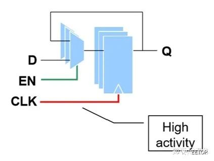
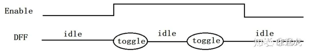
Register-level clock gating is aimed at reducing unnecessary clock flips.
The diagram below illustrates a case where clock gating is not done well; the clock is still enabled during the idle state of the DFF.
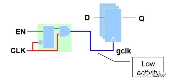
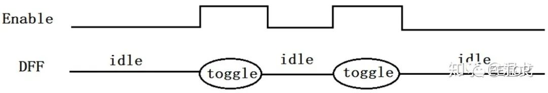
To save power consumption, we can set the enable signal to 0 when the DFF is idle, thus controlling the clock flip and achieving power savings, as shown in the figure below:
When performing clock gating, two points should usually be noted:
1) Currently, registers with large bit widths are often added with gater
Because adding gater itself will also increase area and power consumption, a comprehensive consideration is necessary. For example, if it’s a one-bit register, the power saved by adding a gater may not be worth the power consumption of the gater itself, so it is not worthwhile.
2) After adding a gater, we must ensure that the original circuit functionality remains unchanged.
b. Voltage domain-based low-power design
Voltage is closely related to power consumption. Therefore, power reduction can consider using a lower voltage. There are three ways to implement multi-voltage design technology:
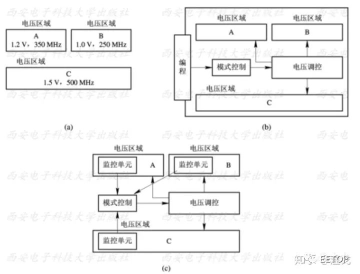
A: Each voltage region has a fixed voltage, as shown in the above figure (a);
B: Each voltage region has multiple fixed voltages, determined by software; as shown in the above figure (b);
C: Adaptive method, where each voltage domain has variable voltages, determined by software; as shown in the above figure (c).
A is fixed voltage allocation, while B and C involve dynamic voltage management, requiring software-hardware co-design.
This brings us to the DVFS technology: Dynamic Voltage Dynamic Frequency Scaling, a method to reduce power consumption in different circuit modules by lowering their operating voltage and frequency to just meet the system’s minimum requirements.
The maximum clock frequency in a circuit module is closely related to voltage. If a circuit can estimate how much work it needs to do to complete the current task, theoretically, it can lower the clock frequency to just enough to complete the task in a timely manner. Lowering the clock frequency allows for a reduction in supply voltage. When both frequency and voltage are lowered, power consumption is greatly reduced. This is the principle of DVFS.
DVFS technology is a form of dynamic voltage management that can be realized through software and hardware methods.
c. Using different threshold library files (Multi-threshold libraries)
As shown in the figure below, if you want the MOS transistor to conduct, the low-threshold cell requires a lower conduction voltage, so it conducts faster than the high-threshold cell, while also having higher leakage.
Therefore, when synthesizing or performing physical design (PD), one must consider strategies to balance speed and power consumption.
d. RTL design
When doing RTL design, we still have ways to save power consumption. For example:
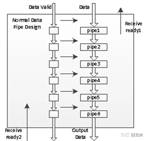
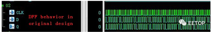
The figure below is a typical pipeline design. When it is in working mode, each register is toggling under the drive of the clk.
This is the simulation waveform of its netlist:
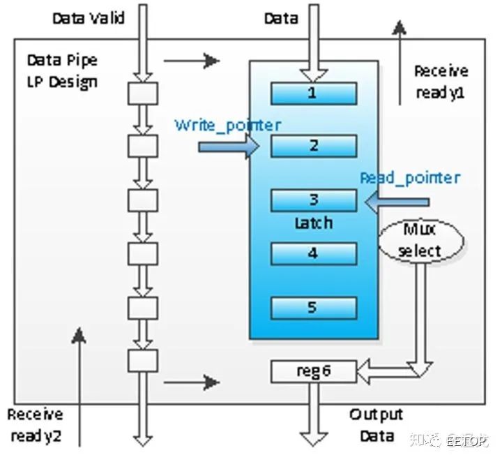
At this time, we can make some improvements to the design, such as using a write_pointer and read_pointer. In a normal pipeline, data is transmitted one bit at a time. After improvement, the pointer moves while the pipeline data remains stationary, thus reducing the number of register toggles. The behavior of this circuit is more like RAM, and we can even use a latch array since latch arrays take up less area.
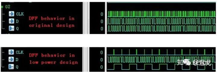
The simulation waveform after the improvement shows that the toggling at the Q end has been greatly reduced.
Below are commonly used tools for power analysis: PTPX/Power Artist
-
PTPX
-
Power Artist / Power Pro
In conclusion: Nothing is free; often reducing power consumption will inevitably affect other aspects, such as area, performance, etc.
Power optimization should also be targeted; for example, desktops may focus more on performance, while mobile phones need a balance between performance and power consumption. Therefore, targeted balancing must be done for different products.
-
Summary of ASIC design learning on low-power design overview and book recommendations
-
Razavi Low–Power SERDES Design PPT sharing
-
Low power RTL design optimization, making your design consume less power under the same process!
-
Top global chip experts reveal the truth about low-power chip design
-
Talking about chip power consumption
Welcome to add us as a star
Due to recent changes in WeChat public account push rules, if you want to frequently see our articles, we recommend marking EETOP as a star. The method is as follows: enter the public account homepage, click the upper right corner “three dots“, then click “set as star“. A yellow star will appear next to our public account name as shown in the figure below:
Add us on WeChat