Table of Contents
【CH.1】What is DRAM? Why is it important?【CH.2】Basic unit of DRAM: Capacitor, Transistor, and Storage Principle【CH.3】Column Address, Address Bus, and the Need for Address Multiplexing.【CH.4】RAS (Row Address Strobe), CAS (Column Address Strobe), WE (Write Enable).【CH.5】Step by Step, with Delay Explanation (RAS-to-CAS Delay, CAS Latency).【CH.6】Step by Step, explaining how data is written and refreshed.【CH.7】Why DRAM must be refreshed (data will disappear).【CH.8】A one-sentence summary of how DRAM works.
What is DRAM? Why is it important?
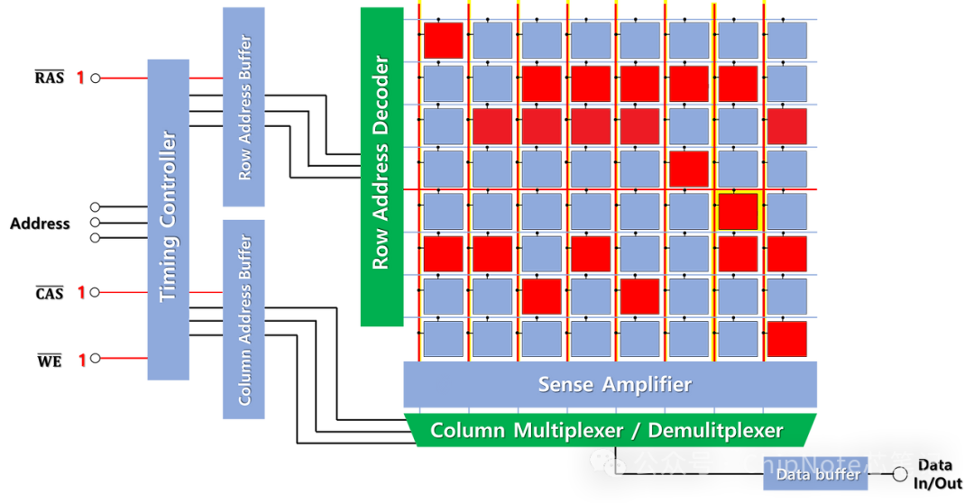
Dynamic Random Access Memory (DRAM) consists of billions of cells, each arranged in a rectangular array containing a transistor and a capacitor. When electrons accumulate on the capacitor, it records a “1”, and when it discharges, it records a “0”. Each transistor is connected to a horizontal Word Line and a vertical Bit Line. The word line controls the transistor’s gate on/off, while the Bit Line is responsible for reading/writing data. To simplify the circuit, we will focus on the components supporting an 8 x 8 memory Array.
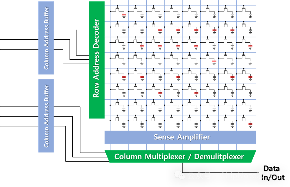
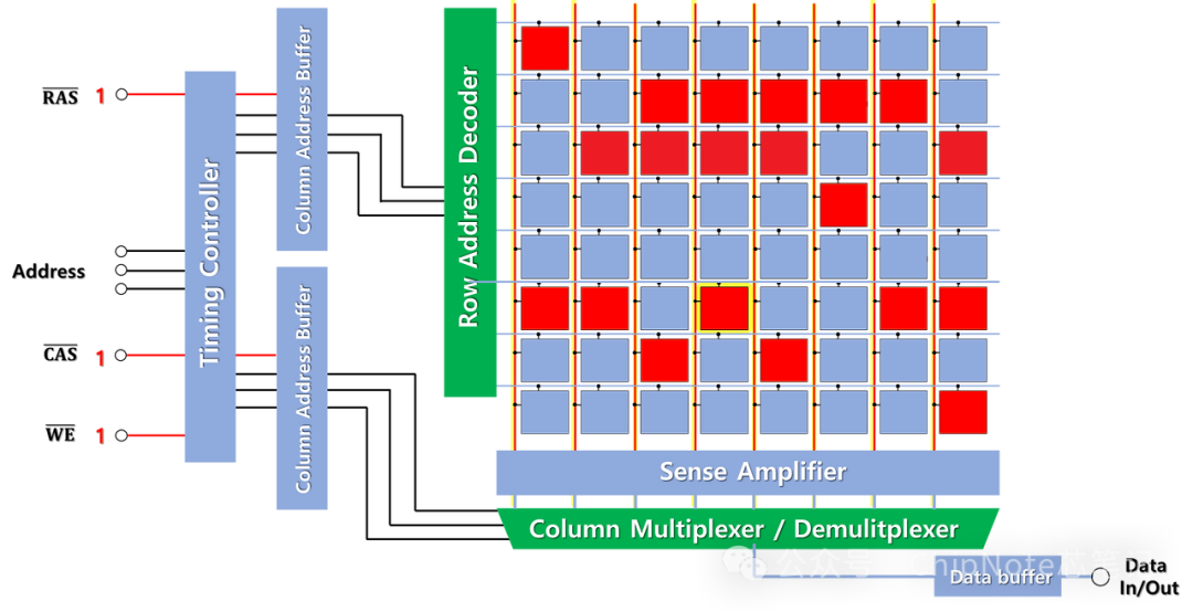
The above image shows an 8×8 memory array. As mentioned, the areas with red boxes on the Capacitor indicate where electrons are charged, identifying data as “1”. First, let’s look at the read and output steps of DRAM. To identify a specific memory address, a portion of the components running together is illustrated.
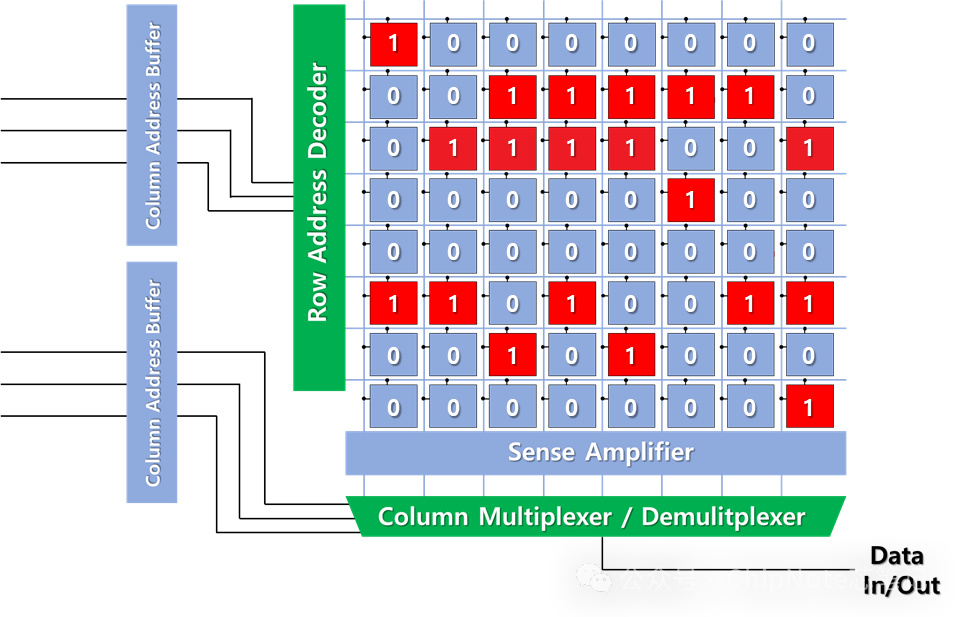
Each cell has a corresponding memory address, and to transmit the memory address, a total of 64 cells in the 8×8 cell array require an Address bus. (2^6=64) A total of 64 binary values is the exact number needed to uniquely identify each cell in the 8×8 Array. Three lines of the Address bus are provided to a latch group known as the Row address buffer, which is connected to the Row Address Decoder. The binary values transmitted by the three address lines uniquely identify a specific row in the cell array, hence this value is referred to as the “row address”.
The other three lines of the Address line are provided to a latch group known as the Column Address buffer. As shown, it connects to the Column multiplexer & demultiplexer. The binary values transmitted by these 3 Address lines can uniquely identify a specific column in the Array. As the name suggests, the latches that make up the Column and Row address buffers temporarily store the row and column addresses.
Column & Row address buffers allow the row and column addresses to be input separately into the memory module due to a system known as memory address multiplexing. Without a multiplexing system, there would need to be many external pins in a memory chip with billions of memory cells. Thus, keeping the number of external pins low is crucial in high-capacity memory with more Memory Addresses. A 6-bit memory address can be managed with just 3 external pins. A 32-bit memory address requires 16 address pins. Generally, DRAM has a very high number of data pins.
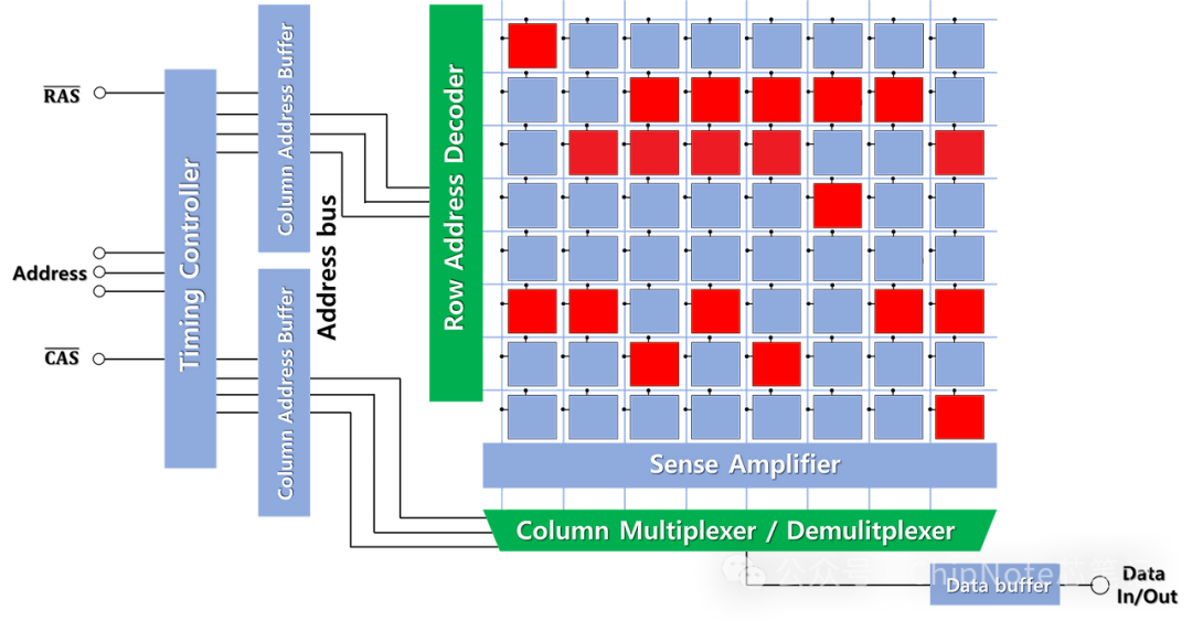
External pins are used not only for transmitting memory addresses and data but also for transmitting power and various control signals. For example, each buffer requires additional pins, such as RAS and CAS. When inputting the Memory address, RAS is the row address strobe, and CAS is the column address strobe. Here, Strobe refers to the signal used to specify the address when accessing DRAM. Generally, DRAM divides the entire Address bus into two parts, accepting row addresses and column addresses separately. In computer memory technology, RAS is the signal sent to DRAM to inform it of the relevant row address. The data bits of DRAM are stored in a cell located at the intersection of the row and column addresses. CAS is the signal sent to confirm the active row address.
[Detailed Explanation] RAS, CAS
Memory has an address structure composed of a matrix of cells arranged in rows and columns, used to store (Write) information or read (Read) stored information. When the processor reads or writes information in memory, it first sends the RAS signal to the row, then sends the CAS signal to the column to confirm the Address. The CAS is responsible for determining whether the memory address contains data. After the CAS signal disappears, new information is re-stored in the Memory address.
Let’s briefly explain the action process of memory.
1. The CPU requests data from the motherboard chipset, which then sends the row address of the memory location containing the data to the memory. This requires one cycle (Hz).
When the row address enters the Row address buffer, the Sense Amplifier reads all cells in that row. The signal resulting from reading these row parts is called RAS, and the time required to read is referred to as RAS-to-CAS delay (the delay time between RAS and CAS). This process takes 2-3 cycles.
3. With just the row address, it is not possible to know where the required data is located. Therefore, ten addresses are received this time. The CAS signal will be sent out to find the exact heat. The time required for this is called CAS latency (CAS delay time). This also takes 2-3 cycles.
4. Using the transmitted row address and heat address, the location of the data is found. The contents of the memory cell are passed to the Output buffer (or data buffer), requiring one cycle.
5. Finally, the motherboard’s chipset reads the contents of the output buffer and passes it to the CPU. This requires one cycle and two cycles respectively.
*CAS latency refers to the time it takes to send the signal to the DRAM to inform the computer storage device of the hot address needed for data processing. After the signal reaches the DRAM, the time required for data processing is measured in clock cycles.
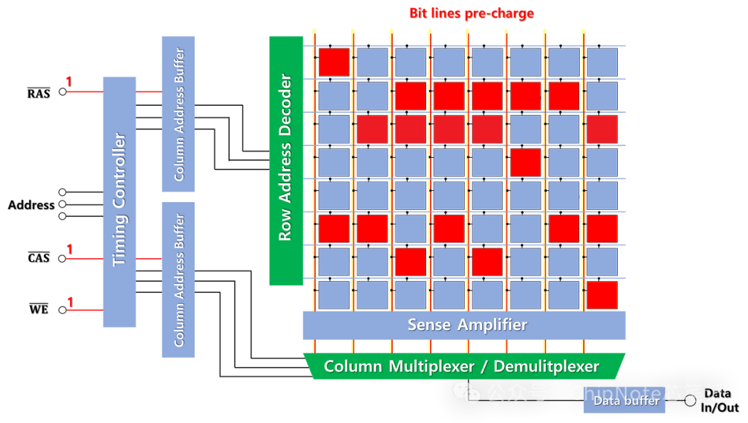
During the read process, the Bit line includes a pre-charge phase, approximately half of the DRAM module’s supply voltage, 1/2Vdd.
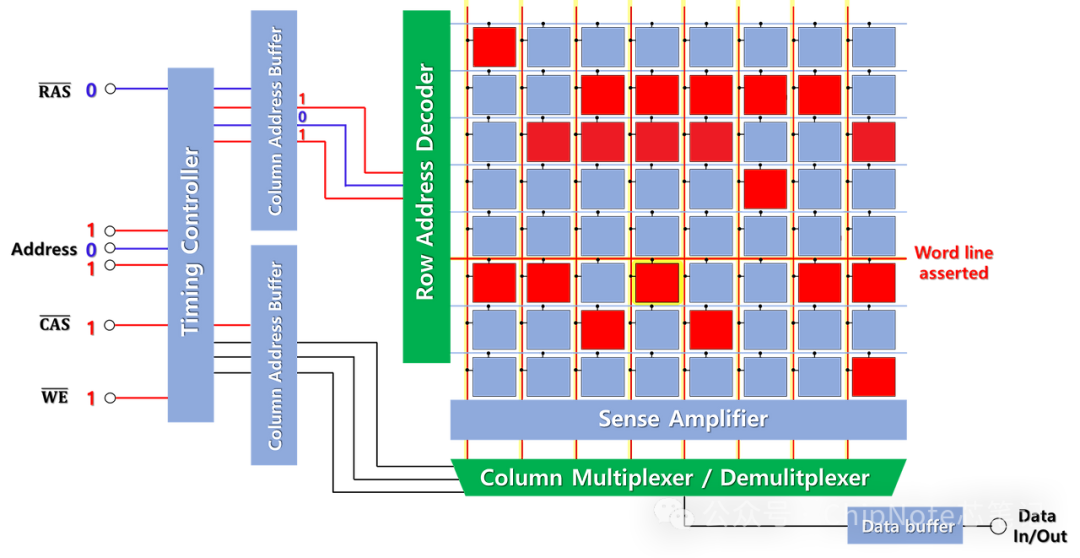
The computer’s Memory controller transmits the Row address to the pin, while RAS is activated simultaneously. The Bit line is separated from the pre-charge circuit, and the decoded row address is lifted. In the above image, the decoder uses a 3-bit memory address to select one from 8 possible outputs and applies voltage to the selected word line. The cell values of the entire row are latched to the sense amplifier. At this point, it also includes the cell we want to read. Reading the value of the Cell is a destructive process; in the cells of all rows containing the required cell, the cells with a value of “1” are partially discharged, while those with a value of “0” are charged. Nevertheless, as shown in the following image, the existing data of the cell is safely latched to the sense amplifier. (The ‘latch’ will be processed later in the circuit, but can be considered as storing just 1 bit.)
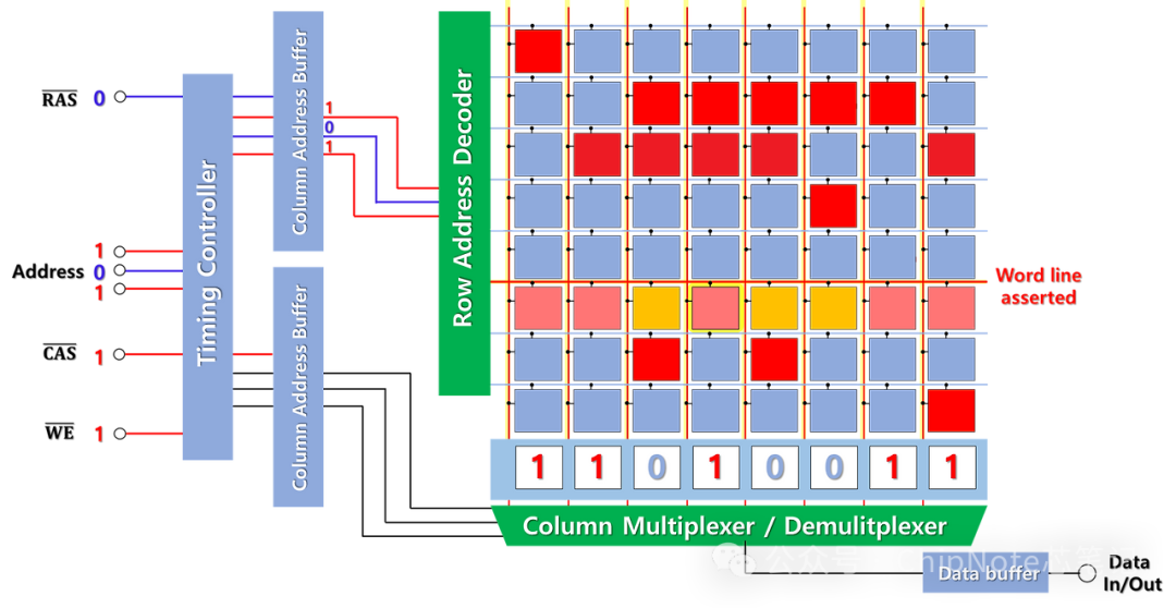
In the memory controller, after the column address is input to the column pins, CAS is activated, and the column address is latched into the column address buffer. The column address selects an appropriate output value in the sense amplifier multiplexer. As shown, the possible input values of the column multiplexer are 8, one of which is the output selection value. At this point, the output value moves to the data buffer, outputting the data of the Cell.
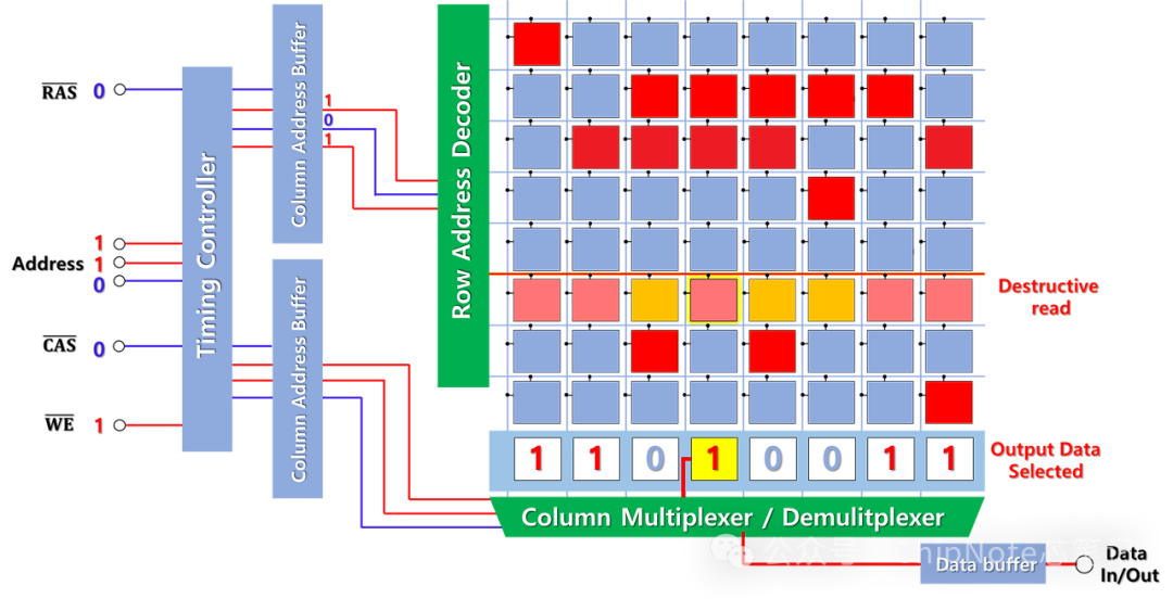
Row Address Strobe, RAS is disabled, and the output external data pin is available. In the last stage of the read cycle, the data from the sense amplifier is used for refresh row operations. Meanwhile, the Column address strobe, CAS, is disabled.
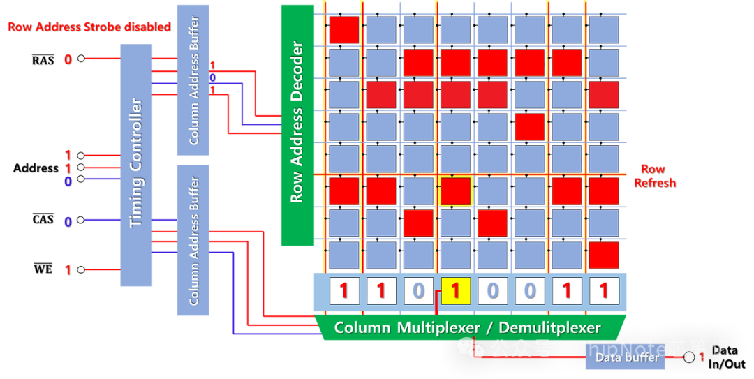
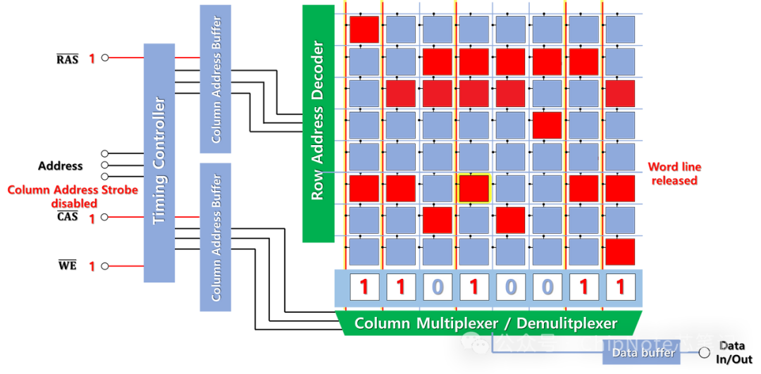
If the word line becomes inactive, the output data can no longer be used. The remaining task is to prepare for the next working sequence of DRAM, performing pre-charging on the bit line. The read cycle requires split-second timing. During the read cycle, some other tasks may occur simultaneously, so waiting for other tasks to take their turn is necessary. Ultimately, the faster the cycle, the better, but having accurate 1 bit is also very important.
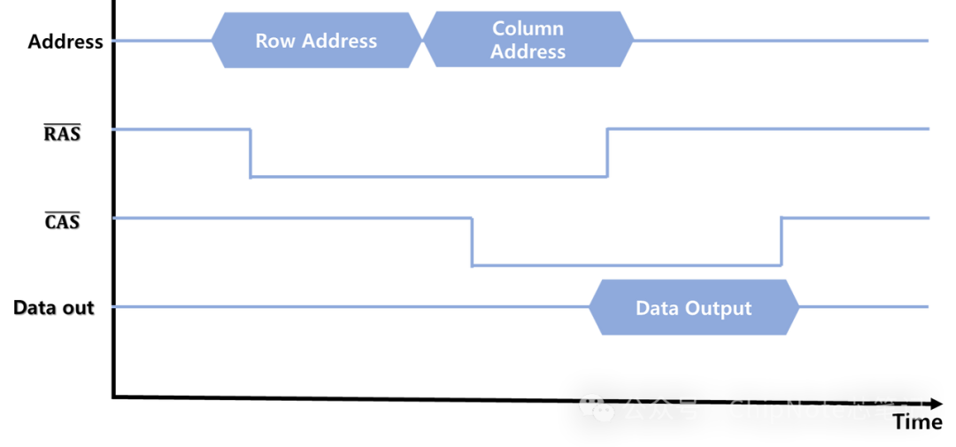
The read cycle can be illustrated using the above diagram. The Row address is transmitted to the external address pin. After that, the Row Address Strobe, RAS, is activated. Then, the Column address is transmitted from the external pin. To allow for signal delay, a short time is permitted, and CAS is activated. After RAS is disabled, data can be output. At this point, the Data output can be used until CAS is disabled. This concludes the Read cycle.
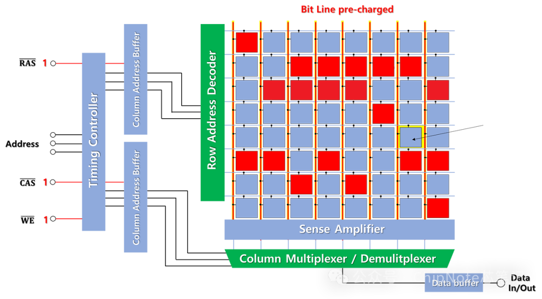
The Write cycle also has a similar structure. As mentioned, I want to write data into the cell displayed in the DRAM module. For example, suppose I want to write “1” onto the cell currently representing “0”. The Bit line is in a pre-charged state. The appropriate Row address is transmitted to the address pin via the memory controller.
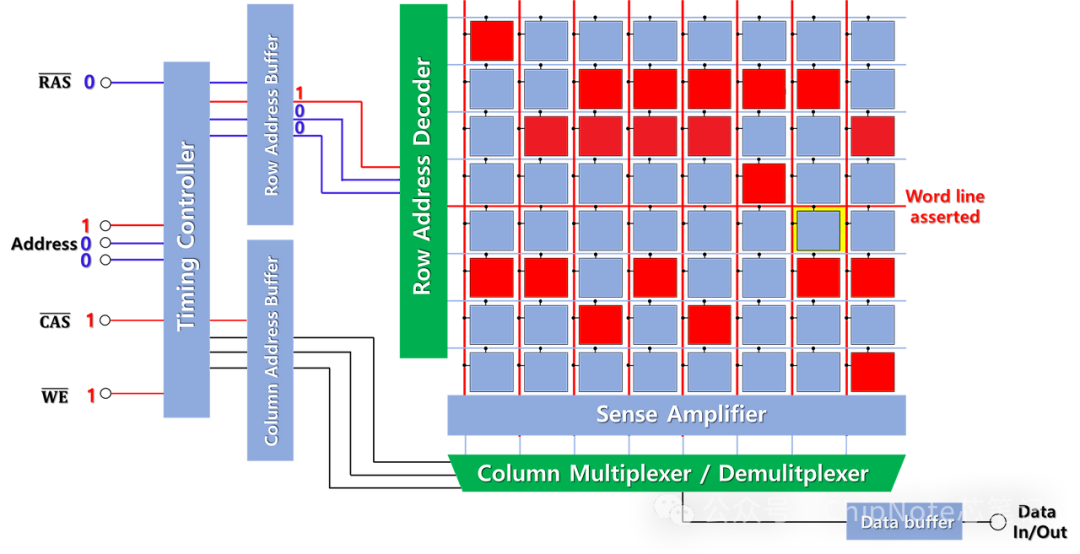
The signal received by the external pin is transmitted to the Row Address Buffer through the controller and decoded. Subsequently, the word line containing the target cell is energized, selecting that row.
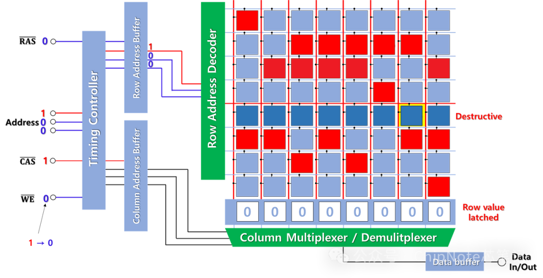
Then, similar to the previous Read cycle, the Row values are latched in the sense amplifier. The read cycle and this process are the same, but at this stage, the input segment applies a writable signal.
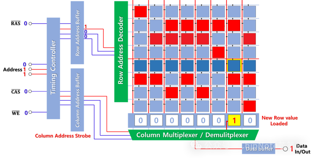
After applying the writable signal, the input side transmits “1” data, activating the Column Address strobe, searching for the corresponding cell to be used. This is how the new Value is loaded into the Sense Amplifier based on the column address in the Column Demultiplexer.
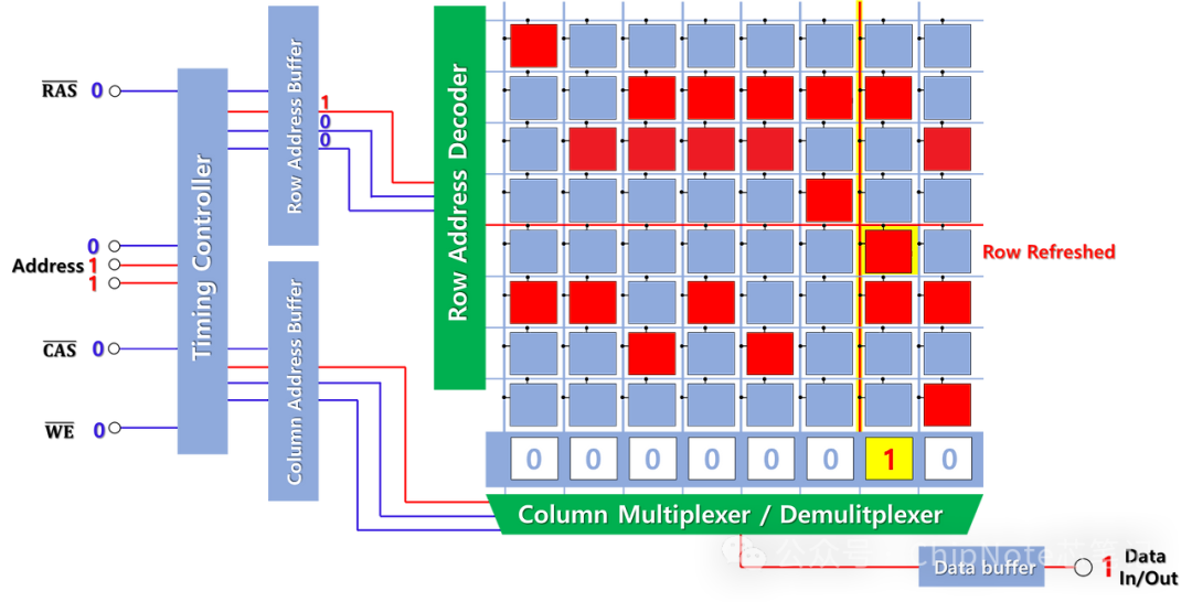
Then, the row will refresh as before, storing the information of “1” in the Cell.
After the refresh, the activation of the input segment on the right side is disabled, and the order of disabling follows the Row Address Strobe, RAS, and Column Address Strobe, CAS. The Bit Line is restored to the Pre-charged state.
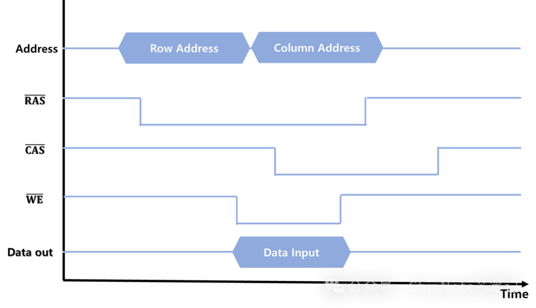
As seen above, let’s look at the sequence diagram of the Write cycle. If the Row address is first transmitted to the address pin, considering signal delay, a short time error is allowed, and RAS is activated. After that, the Column address is also transmitted to the address pin. After the WE signal is activated, the Input data can be used, and CAS will be activated. After WE is disabled, the Input data can no longer be used, and finally, the order of disabling follows RAS and CAS.
Recommended Reading
【Second Communication Chip】5G Era Innovation: The Rise of Next-Generation RF Chips POI-SAW and TF-SAW, Challenging the Dominance of Traditional SAW/BAW Filters!
【Semiconductor Photoresist Materials】Mask Plate Reticle & Photo Mask Uses and Production Process
【Semiconductor Lithography Process】Full Process Lithography Optical High NA Principles, DOF, Process Sequence, Resolution, Wavelength, Pre-bake and Post-bake, Introduction to EUV Process
【Semiconductor Yield】What is Yield? Process Control Techniques for Improving Yield
【Semiconductor Yield】Does Process Shrinking Necessarily Improve Yield? – Understanding Defect Density Used for Yield Prediction
【Semiconductor Cleaning Process】Essential Knowledge Points and Required Cleaning Process Q&A for Semiconductor Production Steps
【Semiconductor Etching Process】The Soul of Semiconductors: From 0 to 1 Teaching Etching Process and Defect Rate Issues for Engineers
【Semiconductor Process】TSMC 2nm Process and Advanced Packaging
【Semiconductor Photoresist Materials】i-line vs DUV vs EUV Photoresist Key Parameter Comparison
【Semiconductor Yield】What is Yield? Process Control Techniques for Improving YieldTH