According to executives interviewed exclusively by EE Times, startup chip manufacturers Celestial and OpenLight are set to produce their first chips this year, providing faster photonics and lower power consumption for large-scale customers running AI data centers, such as Amazon, Microsoft, and Google.
In August, Celestial secured $255 million in funding from TSMC’s VentureTech Alliance and Samsung Catalyst Fund, bringing its total funding to $520 million. Similarly, in August, OpenLight raised $34 million from investors including Juniper Networks (now part of HPE) and Lam Capital, the corporate venture capital arm of Lam Research.
By next year, Celestial plans to sell its first chips, including the company’s Photonic Fabric, a technology that provides optical interconnect networks from chip to chip within processor packages, or from server to server across data center racks. With the soaring demand for next-generation AI infrastructure, Celestial will leverage the new funding to strengthen its supply chain and deepen collaborations with foundries, including TSMC.
OpenLight will use the new capital to expand its active and passive photonic device PDK library, manufactured by foundry Tower Semiconductor, which includes modulators capable of 400 gigabits per second (Gbps) and indium phosphide technology for heterogeneous integrated lasers on chip.
Celestial’s COO Preet Virk told EE Times, “Hyperscale vendors plan to adopt our solutions as soon as we can deliver them, likely in the second half of next year. This includes hyperscale vendors and semiconductor companies for which we provide some interesting solutions.”
OpenLight’s CEO Adam Carter stated that production will begin this year, and he told EE Times that the company has some “significant” customers interested in adopting indium phosphide for co-packaged optical devices (CPO) and other applications.
Carter remarked, “The total bandwidth generated by a CPO will be enormous, much larger than anything anyone else is promoting.” He also added that the company plans to start production for its first customers by the end of this year.
Virk stated, “Hyperscale companies are eager to adopt optical technology.”
Celestial focuses on “vertical scaling” networks within servers, which account for 85% of data center traffic. Virk noted that last year, sales of vertical scaling networks surpassed those of copper-based Ethernet horizontal scaling switches. Other competitors in the photonic chip space include Ayar Labs, Lightmatter, and Huawei.
In March, Lightmatter announced the launch of the Passage M1000, which has a total optical bandwidth of up to 114 Tbps. The M1000 reference platform is a multi-mask active photonic interposer that connects large chips in 3D packages, providing connectivity for thousands of GPUs. Lightmatter has partnered with GlobalFoundries and chip packaging company Amkor to begin customer designs based on the M1000.
Ayar Labs and Alchip Technologies formed a partnership in September to combine Ayar’s CPO and Alchip’s design expertise with TSMC’s compact optical universal photonic engine (COUPE) advanced packaging technology.
According to Celestial, as major companies race to build AI computing capabilities, the largest infrastructure investment in history is underway. Companies like IBM are also joining the competition. Quantum computing startup PsiQuantum has manufactured photonic chips using standard 45-nanometer silicon nitride processes at GlobalFoundries’ facility in Malta, New York.
Celestial’s CEO David Lazovsky stated in a statement, “The AI industry is facing a fundamental bottleneck, where data is transmitted between AI processors via copper wires. Current copper-based interconnects cannot scale efficiently to meet the demands of millions of processors required for next-generation AI.”
Challenging Nvidia’s NVLink
Celestial claims that its photonic architecture significantly outperforms Nvidia’s NVLink in terms of power consumption. NVLink interconnects enable faster and more direct communication between GPUs compared to traditional PCIe.
Virk stated, “When communicating from GPU to GPU, we consume only a quarter of the power of an NVLink switch.”
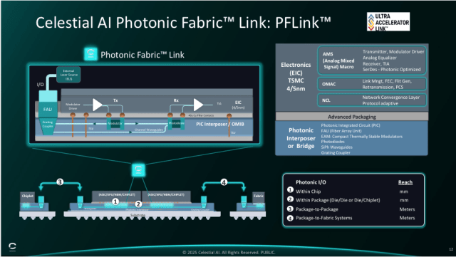 Source: Celestial
Celestial is launching its patented Optical Memory Interface Bridge (OMIB) as an alternative to NVLink. OMIB is similar to advanced packaging technologies such as Intel’s EMIB, TSMC’s CoWoS, and Samsung’s IQE. OMIB provides photonic connections both within the chip and between other chips. Celestial’s control circuit’s transmit/receive sections utilize TSMC’s 4-nanometer and 5-nanometer processes.
Huawei also targets NVLink
Huawei’s rotating chairman Xu Zhijun stated that this week, the company launched a new SuperPod cluster that will connect up to 15,488 Ascend NPUs and operate them as a coherent system. The SuperPod product will be applied to Huawei’s Ascend chips next year.
EMI Challenges
“If you look at the roadmaps of Nvidia and AMD, you’ll see they are integrating large full-mask chips into a single package,” Virk said. “Connecting these chips with high-speed, high-density interconnects within the package is becoming a significant challenge for EMI signal integrity. We can place optical IO anywhere on the chip. Currently, every chip produced in the world has optical IO located at the edge of the chip. We don’t have that problem because our modulators are not as thermally sensitive as micro-rings.”
Celestial does not use micro-rings but instead employs EAM (electro-absorption modulators) to modulate light absorption by applying an electric field, thereby controlling the intensity of the laser beam.
Virk stated, “Currently, an operation by Nvidia takes 600 to 700 nanoseconds, while we can complete it in 100 to 200 nanoseconds with very low power consumption, about 2.8 picojoules per bit.”
OpenLight’s Carter stated that his company has achieved approximately 1.5 picojoules/bit transmission efficiency using its 200 Gbps modulators. “If we now scale using the same DFB (distributed feedback laser) and replace the 200 Gbps modulator with a 400 Gbps modulator, the transmission efficiency per bit can essentially be halved due to the smaller voltage increase. This is the inherent advantage of heterogeneous integration.” The company announced a 400 Gbps modulator in February.
“We have successfully demonstrated a 400 Gbps modulator based on indium phosphide,” Carter said. “This means customers can scale and horizontally expand their networks for greater bandwidth and higher density.”
About Packaging
Carter stated that the focus of competition is advanced packaging.
“Many companies have different requirements when announcing CPO or modulation, especially regarding packaging, what is inside the package, what the dimensions are, and what the scale looks like.
It will not initially be based on standards. OpenLight’s positioning is very unique because we do not necessarily manufacture chips for you. We provide you with a component library so you can design your own chips.
OpenLight is collaborating with chip packaging company ASE’s subsidiary ISE located in California. Celestial aims to provide its proprietary chip set to chip designers after mass production. “One way to do this is to provide you with a set of optical chips that need to be packaged,” Virk said. “This optical chip set comes with an EIC (Embedded Interposer Carrier).”
EIC is a new packaging technology that acts as an embedded interposer, integrating chips into a multi-layer package similar to SOC, at a lower cost than traditional 3D ICs. Virk stated, “We provide you with chips along with all packaging and optical technology, and you can go to any OSAT for packaging.” As an alternative to chips, Celestial also plans to apply its IP to customer chips.
The company is currently wafer-fabricating, and Virk believes this is the world’s first large SoC equipped with optical IO in the middle of the chip.
Celestial’s Senior Director of Product Management Ravi Mahatme stated, “We place the memory controller at the edge of the chip. On the south edge of the chip, we place two HBM controllers for HBM3e. On the east and west sides, we place four DDR controllers to address eight DDR DIMMs. Through software, HBM can act as a cache for DDR. This essentially hides the memory access latency of DRAM.”
Mahatme stated that this development will be a game changer.
“This is a unified memory space where any processor can read and write to any memory location,” he said. “The size of DLRM (Deep Learning Recommendation Model) reaches terabytes. Currently, the only way to store these models is to connect XPUs together. This changes the game because this model can be stored locally.”