Abstract
At intersections, vehicles shuttle, pedestrians bustle, with orderly lanes for vehicles and sidewalks for pedestrians. What ensures this orderly flow? It is the automatic control system of traffic lights. There are many control methods for traffic lights. This design is mainly divided into five major modules: input control circuit, clock control circuit, internal and external program switching control, and display circuit. The design centers around the MSC-51 series microcontroller, Intel AT89C51, to create a traffic light controller, implementing the function of setting the red, green, and yellow light durations through the P0 port of the AT89C51 chip. To ensure system stability and reliability, a debouncing circuit using the 74LS14 Schmitt trigger chip is employed to avoid erroneous operations caused by signal jitter. The display time is directly output through the P2 port of the AT89C51, driven by the CD4511 to show the red light duration on an LED digital tube.
Keywords: AT89C51, LED display, traffic light
Introduction
This course design is a comprehensive application of the knowledge learned in the microcontroller principles course, culminating in the design and implementation of a microcontroller application system in the laboratory. The main task of this design is to consolidate and deepen the theoretical knowledge and experimental skills learned in the “Microcontroller Principles and Applications” course by solving one or two practical problems, mastering the general design methods of microcontroller application circuits, enhancing the design and experimental capabilities of electronic circuits, deepening the understanding of microcontroller hardware and software knowledge, and gaining preliminary application experience to lay a solid foundation for future work.
Today, traffic lights are installed at various intersections and have become the most common and effective means of managing traffic flow. However, this technology emerged in the 19th century. The advent of traffic signals has allowed for effective traffic regulation, significantly improving traffic flow, increasing road capacity, and reducing traffic accidents. After three weeks of study, I have gained a preliminary understanding of the structure and function of microcontrollers. Microcontrollers play a crucial role in traffic control, and mastering their working principles essentially leads to an understanding of how traffic lights operate. As a student, to better grasp the structure and function of microcontrollers and to further enhance my practical skills, I have designed the following traffic light system.
Project Overview
(1) Overview
This design is an experimental control of traffic lights, which requires an understanding of the actual traffic light change patterns. Assume an intersection oriented east-west and north-south, with the initial state being zero, where all lights are off. Then, transition to state one where the east-west green light is on, and the north-south red light is on. After a period, transition to state two, where the east-west green light flashes a few times before turning yellow, with a delay of a few seconds, while the north-south remains red. Next, transition to state three where the north-south green light is on, and the east-west red light is on. After a period, transition to state four where the north-south green light flashes a few times before turning yellow, with a delay of a few seconds, while the east-west remains red. Finally, cycle back to state one. The traffic signal simulation control system design utilizes the microcontroller’s timer to control the alternating illumination and extinguishing of the red and green lights at the intersection, and uses an LED digital tube to display the time. However, due to time and skill limitations, the time is not displayed in this experiment. Twelve light-emitting diodes are used to simulate the traffic lights for the experimental design.
This design is a comprehensive training for the “Microcomputer Interface and Control Technology” course. Through theoretical learning, topic selection, literature review, software and hardware design, and system debugging, we consolidate the knowledge learned and improve application levels. Here, we learn to apply scientific methods from problem identification, observation, and analysis to ultimately solving problems, enhancing our thinking and practical abilities, gaining hands-on experience in design, and cultivating our work style and attitude. This lays a solid foundation for future graduation projects and for engaging in the design and maintenance of microcomputer control systems.
The significance of this project design lies in mastering the general methods of microcomputer control system design and problem-solving approaches through the design of a specific control system, especially some commonly used technical means. This allows us to accumulate design experience in a practical teaching environment, expand our thinking space, and comprehensively improve our overall capabilities.
(2) Process Flowchart
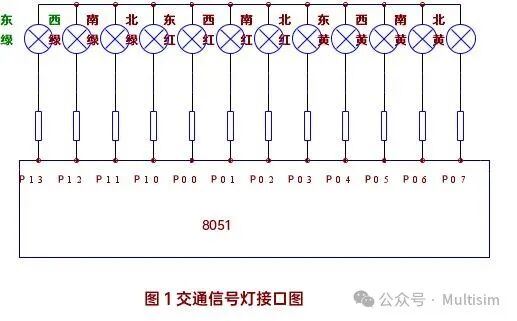
Since this experiment is a traffic light control experiment, it is necessary to first understand the actual traffic light change patterns. Assume an intersection oriented east-west and north-south. The initial state is zero, where all lights are off. Then transition to state one where the east-west green light is on, and the north-south red light is on. After a period, transition to state two, where the east-west green light flashes a few times before turning yellow, with a delay of a few seconds, while the north-south remains red. Next, transition to state three where the north-south green light is on, and the east-west red light is on. After a period, transition to state four where the north-south green light flashes a few times before turning yellow, with a delay of a few seconds, while the east-west remains red. Finally, cycle back to state one. The traffic signal simulation control system design utilizes the microcontroller’s timer to control the alternating illumination and extinguishing of the red and green lights at the intersection, and uses an LED digital tube to display the time. However, due to time and skill limitations, the time is not displayed. Twelve light-emitting diodes are used to simulate traffic light management. The specific interface is shown in Figure 1.
Project Design
(1) Determining the Control Scheme
The principle of the traffic light control system mainly consists of the controller, timer, decoder, and second pulse signal generator. The second pulse generator serves as the standard clock signal source for the timer and controller in this system, while the decoder outputs two sets of control signals for the traffic lights, which are then driven by the driving circuit to operate the lights. The controller is the main part of the system, controlling the operation of the timer and decoder. As shown in Figure 2, the complete circuit board.
Figure 2 Complete Circuit Board
(2) Hardware Section
(1) Hardware Design of the Traffic Light Control System:
The hardware design of the traffic light control system includes: memory expansion (62256), I/O port expansion (8255), address latching (74LS373 or 74LS273), and inverters (7407).
The data buffer, I/O control logic, control and timing registers, timing and control circuits, scanning counters, response buffers, FIFO/sensor RAM and its status registers, display RAM and display address registers, etc., are all components of the system.
(2) The hardware system design adheres to the following principles:
1. Meet the design requirements of the system and be easy to operate and maintain.
2. The system functions flexibly and is easy to expand.
3. It has automatic diagnostic capabilities.
(3) Hardware Structure Block Diagram (as shown in Figure 3).
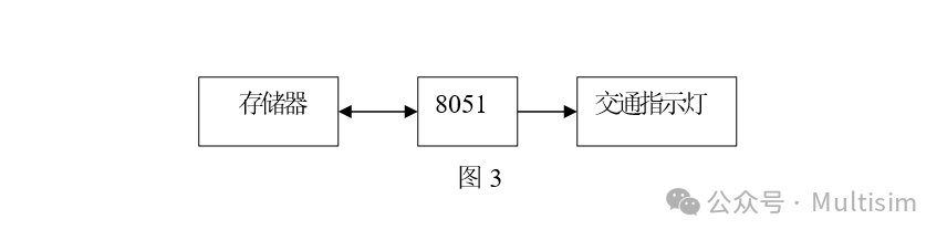
The hardware system in this system mainly serves to transmit data, perform logical calculations, and provide displays, as well as allow for manual data modifications, system startup, stopping, etc. Additionally, the safety and reliability of system operation depend on the hardware system.
(4) Principle Block Diagram of the Traffic Light Control System (as shown in Figure 4).
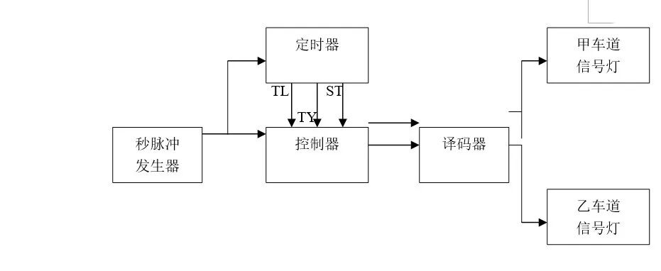
Figure 4 Principle Block Diagram of the Traffic Light Control System
In the diagram:
TL: Indicates that the green light interval for lane A or lane B is 25 seconds, which is the normal passage time for vehicles. When the timer reaches the set time, TL=1; otherwise, TL=0.
TY: Indicates that the yellow light interval is 5 seconds. When the timer reaches the set time, TY=1; otherwise, TY=0.
ST: Indicates that after the timer reaches the specified time, the controller sends a state transition signal, controlling the timer to start timing for the next working state.
1. Timer
The timer consists of a counter synchronized with the system’s second pulse (provided by the clock pulse generator), requiring the counter to be cleared under the action of the state signal ST, and then, under the rising edge of the clock pulse, the counter starts counting from zero, providing the control signals TY and TL for timing mod 5 and mod 25, respectively (the circuit diagram is shown in Figure 5).

Figure 5 Timer Circuit Diagram
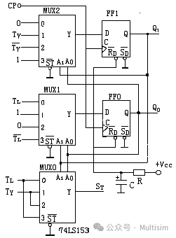
2. Controller
The controller is the core of traffic management, and it should be able to control the state transitions of the signal lights according to traffic management rules. From the ASM diagram, the state transition table of the controller can be listed, as shown in Table 1. Two D flip-flops FF1 and FF0 are selected as the timing registers to generate four states, and the conditions for state transitions of the controller are TL and TY. When the controller is in the state Q1n+1Q0n+1=00, if TL=0, the controller remains in the 00 state; otherwise, the controller transitions to the state Q1n+1Q0n+1=01. These two cases are independent of the condition TY, so they are represented by the don’t care term “X” (the controller logic diagram is shown in Figure 6).
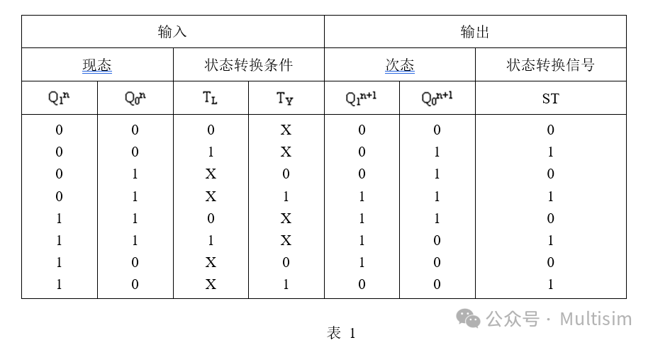
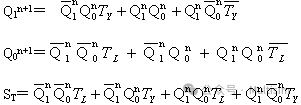
Based on Table 1, the state equations and transition signal equations can be derived. The method is to AND the input or state transition condition variables corresponding to Q1n+1, Q0n+1, and ST=1, where “1” is represented by the original variable and “0” is represented by the inverted variable, and then OR all the AND terms to obtain the following equations:
Controller Logic Diagram (as shown in Figure 6)
3. Decoder
The 74LS138 decoder has three input terminals, forming eight input states, and has eight output terminals, each corresponding to one of the eight input states, with low-level validity. Additionally, there are three enable terminals E3, E2, and E1, which must all receive valid levels simultaneously for the decoder to operate, specifically E3=1, E2=0, E1=0.
The main task of the decoder is to translate the four working states of the controller’s outputs Q1 and Q0 into the working states of the six signal lights on lanes A and B. The relationship between the controller’s state encoding and the signal light control signals is shown in Table 12,4. Readers are encouraged to design the decoding circuit to achieve the above relationship.
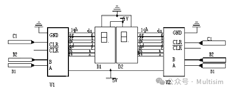
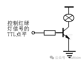
4. Traffic Light Driving Circuit (as shown in Figure 7)
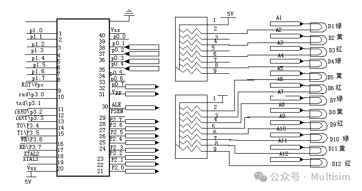
5. Circuit Diagram (as shown in Appendix B) and Circuit Diagram Explanation
Circuit Diagram Explanation
1. This LED dynamic display circuit uses one I/O port P0 of the microcontroller.
2. The lower four bits of the P0 port output display the BCD code of the number, which is sent to the 74LS138 for decoding. The output segment code is then pulled up by a pull-up resistor and sent to the pins of each display segment of the display.
3. The P03, P04, and P05 ports output bit selection signals. The bit selection signals are sent to the 74LS138 for decoding to generate the display’s bit selection signals.
4. When the output short code is generated, the low-level port will pull the level of that port low. Therefore, the LED will not light up, while the high-level port will provide a high level to the anode of the LED. As long as that bit is selected, the LED will light up, and the corresponding number will appear in the segment code table. Each bit selection circuit consists of a PNP transistor. When the bit selection port outputs a low level, the transistor for that bit will saturate and conduct, grounding the display due to the common cathode structure of the display.
5. When the pulse reaches the MCS-51 microcontroller, the 8-bit LED display will receive the signal and store it in the expansion register. When the lower four bits of the P0 port output the BCD code of the number, the output BCD code is sent to the 74LS138 decoder for decoding, and then the display digit is queried in the segment code to show the number.
6. The first four bits display the main road passage time, while the last four bits display the branch road time, controlling the release and prohibition of vehicles through the LED display.
(5) Structure and Pin Functions of 8279:
The internal structure of 8279 consists of a data buffer, I/O control logic, control and timer, timing control circuit, scanning counter, response buffer, FIFO/sensor RAM and its status registers, display RAM and display address registers, etc.
(a) Data Buffer and I/O Control Logic: The data buffer is a bidirectional buffer that connects the internal bus and external bus, used to transfer commands, data, and status between the CPU and 8279. The I/O control logic completes the read and write control of the chip, chip selection, and port selection.
(b) Control and Timer: Used to store operation command words.
(c) Scanning Counter: The scanning counter has two working modes. One is the external decoding mode, where the counter counts in binary, and the four-bit counting state is output from scanning lines SL0-SL3, which is decoded by an external decoder to form a 16-bit scanning signal; the other is the internal decoding mode, where the low two bits of the scanning counter are internally decoded and output from SL0-SL3 to form a four-bit scanning signal.
(d) Response Buffer: The response buffer buffers and latches the response signals from the eight response lines SL0-SL7.
(e) FIFO/Sensor RAM and its Status Register: FIFO/Sensor RAM is a dual-function 8*8 RAM.
(f) Display RAM and Display Address Register: The display RAM is used to store display data, with a capacity of 16*8 bits. During the display process, the stored display data is output from the display register in turn.
In the traffic light control experiment, its chip selection signal line connects to Q0, and the data selection input line connects to Q1, so its control port address is FF82H, and the data port address is FF80H, with the interrupt being suspended.
8051 Minimum Application System
The 8051 is a chip without internal program memory supply status. Therefore, its minimum application system must extend EPROM externally. The address lines A8-A15 of the external program memory are provided by the P2 port; A0-A7 are provided by the P0 port through the address latch. The latch signal for the address latch is ALE. Instruction data is read in through the P0 port. The instruction fetch signal for the program memory is /ALE. Its chip selection line is directly grounded. Additionally, a unit clock circuit must be present.
8255 Programmable Interface Chip
The three parallel I/O ports – Port A, Port B, and Port C are used in this design for Ports A and B.
1) Working mode control circuit;
2) Read and write control logic circuit;
Data bus buffer;
(3) Software Section
(1) Calculation of Delay Subroutine:
Using registers R0, R1, and R2 as counting values, R2 temporarily stores 1, and R1 stores 0. When decremented by 1, it becomes 255, meaning R1 stores 256. R0 stores the number #0B2H, which is 178. The total number of instruction cycles is (see the attached delay program).
DELAY2 delay is:
N=(2+2+2+1+1+2*178)+255*(1+1+2+2*178)=9164.
In total, there are 9164 instruction cycles, and the system crystal frequency is 11.0592. Therefore, T=12/11.0592=1.085 (microseconds).
The delay DELAY2 is:
t=9164*1.085/1000000=0.09996
Approximately equal to 0.1 (seconds).
By changing the value of R2, the delay in seconds can be altered.
(2) Flowchart (as shown in Figure 8)
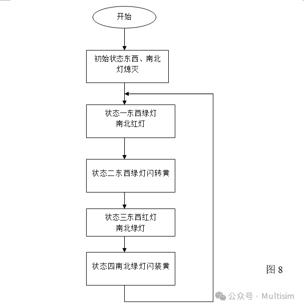
Initially, all lights at the four intersections are off, the east-west green light is on, and the north-south red light is on for a delay of 20 seconds, the green light flashes three times for 3 seconds, then turns yellow for 2 seconds, then the north-south green light is on, and the east-west red light is on for a delay of 20 seconds, the green light flashes three times for 3 seconds, then turns yellow for 2 seconds, and this cycle continues.
(3) Source Program (as shown in Appendix A)
(4) Execution Expression of the Program (as shown in Table 2)
|
State |
Duration/S |
East-West Direction |
North-South Direction |
||||
|
1 |
50 |
On |
Off |
Off |
Off |
Off |
On |
|
2 |
3 |
Flashing |
Off |
Off |
Off |
Off |
On |
|
3 |
2 |
Off |
On |
Off |
Off |
Off |
On |
|
4 |
50 |
Off |
Off |
On |
On |
Off |
Off |
|
5 |
3 |
Off |
Off |
On |
Flashing |
Off |
Off |
|
6 |
2 |
Off |
Off |
On |
Off |
On |
Off |
|
Cycle |
System Debugging and Operation
(1) Hardware Debugging
Using the DVCC experimental and development system, along with basic testing instruments (multimeter, oscilloscope, etc.), to check for faults in the user system hardware. Hardware debugging can be divided into static debugging and dynamic debugging.
(1) Static Debugging
Static debugging is a type of hardware inspection when the user system is not operational.
Step 1: Visual Inspection. Check whether there are any breakpoints in the various external components or circuits.
Step 2: Use a multimeter for testing. First, use the multimeter to verify any questionable connection points found during visual inspection, and then check for any short circuits between various power lines and ground lines.
Step 3: Power-on Testing. Power the board and check whether the power terminals of all sockets or components meet the required values.
Step 4: Online Inspection. Only the microcontroller development system can complete the debugging of the user system.
(2) Dynamic Debugging
Dynamic debugging is a type of hardware inspection that discovers and eliminates internal faults in user system hardware, device connection logic errors, etc., while the user system is operational. The general method for dynamic debugging is to work from the near to the far, and from the part to the whole. The part to whole method means first dividing the user system hardware circuit into several blocks based on logical functions. When debugging the circuit, all unrelated devices are removed from the user system, thus limiting the fault range to a specific local circuit. Once each block circuit is confirmed to be fault-free, each block circuit is gradually added back into the system, debugging the functions of each block circuit and any potential interconnections between circuits. The debugging process from part to whole is then completed. The near to far method involves layering the devices through which the signal flows according to their logical distance from the microcontroller, and then debugging layer by layer. During debugging, the method of removing unrelated components is still used, and the debugging continues layer by layer until the faulty component is located.
System Design and Summary Characteristics
This course design has been immensely beneficial, allowing me to understand and master some programming concepts and the conditions for using and applying I/O ports, as well as the functions of various pins of the microcontroller. It has achieved an effective combination of software and hardware, both of which are indispensable. The design has enabled me to apply theoretical knowledge of microcontrollers in practice, realizing the integration of theory and practice. I have learned that theory is the foundation of practice, and practice can verify the correctness of theory, which has further stimulated my thirst for professional knowledge. This will greatly assist and influence me in my future work or further studies.
This course design has also taught me how to write papers and understand the elements of a thesis, which will be very helpful for my future graduation thesis and will also benefit me greatly in my future work. In writing the paper, I have made significant progress in mastering the basic principles of microcontrollers, the development process of microcontroller application systems, and common programming design thinking techniques, laying a solid foundation for becoming a qualified application-oriented talent.
As a student, in designing the traffic light system, due to a lack of knowledge and experience, I could only complete this design by imitating other programming ideas, along with some of my own thoughts, so there are some shortcomings in various aspects. I welcome corrections. However, I will gradually improve and consolidate my microcontroller knowledge in my future studies.
Thanks
This course design has deepened my understanding of microcontrollers and made me realize their importance in real life. I would like to thank Suzhou University for enabling me to successfully complete the design of the traffic light system. I also owe my gratitude to Professor Hu Danfeng for his help in theory and practice, which allowed me to complete the project successfully and learn a lot. I also want to express my thanks to my classmates who have helped me. In my future studies, I will work even harder to repay the school and teachers for their cultivation.
References
(1) Cao Tianhan. Microcontroller Principles and Interface Technology, Beijing: Electronic Industry Press
(2) Liu Guorong. “Microcontroller Technology”, Machinery Industry Press
(3) Zhou Hui. “Microcomputer Interface and Control Technology” Course Design Guide, Hunan University of Technology Press
(4) “Microcontroller Principles and Interface Technology” Electronic Industry Press
(5) “Microcontroller Technology” Machinery Industry Press
Appendix A: Source Program
ORG 0000H
SJMP A3 ; Four red lights on
A3: MOV SP,#60H
MOV A, #24H
MOV P1, A
CLR P3.4
CLR P3.3
SETB P3.5
SETB P3.2 ; Display for 5 seconds
MOV R4,#05H
LOOP1: MOV R2,#03H
LCALL LP ; Call display subroutine
DJNZ R4,LOOP1
MOV R4,#00H
MOV R2,#03H
LCALL LP ; East-west green light on, north-south red light on
A2: MOV A,#0CH
CLR P3.5
MOV P1,A
SETB P3.3
CLR P3.4
SETB P3.2 ; Display for 20 seconds
MOV R4,#14H
LOOP2: MOV R2,#03H
LCALL LP ; Call display subroutine
DJNZ R4,LOOP2
MOV R4,#00H
MOV R2,#03H
LCALL LP ; Call display subroutine
SETB P3.2
CLR P3.3 ; Display for 5 seconds
MOV R4,#05H ; East-west yellow light on, north-south red light on
LOOP9: MOV A,#14H
MOV P1,A
CLR P3.5
SETB P3.4
MOV R2,#02H
LCALL LP ; Call display subroutine
MOV R2,#01H ; Timing
LCALL DELAY ; Call delay subroutine, north-south red light on
MOV A,#04H
MOV P1,A
CLR P3.4
CLR P3.5
MOV R2,#01H ; Timing
LCALL DELAY ; Call delay subroutine
DJNZ R4,LOOP9
MOV R4,#00H
MOV R2,#03H
LCALL LP ; Call display subroutine, east-west red light on, north-south green light on
A8: MOV A, #61H
MOV P1,A
CLR P3.4
CLR P3.3
CLR P3.2
SETB P3.5 ; Display for 20 seconds
MOV R4,#14H
LOOP3: MOV R2,#03H
LCALL LP ; Call display subroutine
DJNZ R4,LOOP3
MOV R4,#00H
MOV R2,#03H
LCALL LP ; Call display subroutine
SETB P3.5
MOV R4,#05H
LOOP10: MOV R2,#02H
LCALL LP ; Call display subroutine, east-west red light on, north-south yellow light on
A0: MOV A,#0A2H
MOV P1,A
CLR P3.4
CLR P3.3
CLR P3.2
MOV R2,#01H ; Timing
LCALL DELAY ; Call delay subroutine, east-west red light on
MOV A,#20H
MOV P1,A
CLR P3.4
CLR P3.3
CLR P3.2
MOV R2,#01H ; Timing
LCALL DELAY ; Call delay subroutine
DJNZ R4,LOOP10
MOV R4,#00H
MOV R2,#03H
LCALL LP ; Call display subroutine
LJMP A2 ; Delay subroutine
DELAY: PUSH 2
PUSH 1
PUSH 0
DELAY1: MOV 1,#00H
DELAY2: MOV 0,#0B2H
DJNZ 0,$
DJNZ 1,DELAY2
DJNZ 2,DELAY1
POP 0
POP 1
POP 2
DJNZ R2 ,DELAY
RET ; Display subroutine
xian: MOV A,R4
MOV B,#10
DIV AB
MOV R6,A
MOV DPTR,#TAB
MOV A,B
MOVC A,@A+DPTR
MOV SBUF,A
MOV R7,#0FH
H55S: DJNZ R7,H55S
MOV A,R6
MOVC A,@A+DPTR
MOV SBUF,A
MOV R7,#0FH
H55S1: DJNZ R7,H55S1
LCALL DELAY
RET
This is the traffic light subroutine. It mainly controls the on/off status and timing of the lights in each direction.
TAB: DB 0fch,60h,0dah,0f2h,66h,0b6h,0beh,0e0h
DB 0feh,0f6h,0eeh,3eh,9ch,7ah,9eh,8eh ; Lookup table subroutine
END
Appendix B: Circuit Diagram