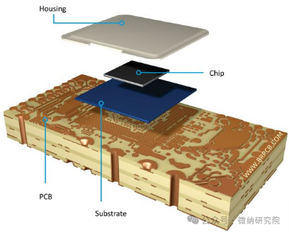
In the semiconductor packaging process, there is a core material that is easily overlooked yet critically important — the IC packaging substrate (referred to as “packaging substrate”). It serves as the bridge connecting the chip and the PCB; without it, the chip’s circuits cannot be connected, and heat cannot be dissipated. Even the most powerful CPU or GPU would remain an unfulfilled product. More importantly, in high-end packaging, the packaging substrate accounts for 70%-80% of the material cost, which is even higher than the cost of the chip’s substrate itself.
 If you wish to stay updated, click above to follow and set as a star!
The packaging substrate is not an ordinary PCB.
Many people equate the packaging substrate with a “mini PCB”, but in reality, its technical requirements and functional positioning are far superior to those of ordinary PCBs. Simply put, the packaging substrate is the “key carrier” for chip-level packaging, undertaking four core functions that are indispensable.
1. Electrical Connection
The most critical role of the packaging substrate is to establish high-density interconnections between the chip (Die) and the PCB — the number of pins on a chip can range from dozens to tens of thousands, and the line width/spacing of ordinary PCBs cannot meet the connection requirements. In contrast, the line width/spacing of packaging substrates can achieve 10-20μm, accurately routing each signal from the chip and avoiding signal interference or disconnection. For example, in flip-chip (FC) packaging, the chip connects directly to the packaging substrate via solder balls, which then connects to the PCB through a ball grid array (BGA), forming a complete signal chain of “chip → substrate → PCB”.
2. Physical Protection and Fixation
The chip itself is a fragile silicon wafer that cannot be directly exposed to the external environment. The packaging substrate provides physical support for the chip: on one hand, it secures the chip to the substrate surface using adhesive materials to prevent mechanical vibrations from causing the chip to fall off; on the other hand, the substrate’s insulating material can isolate external moisture and dust, preventing the chip from getting damp or contaminated, thus extending its lifespan.
3. Thermal Management
When the chip operates, it generates heat; if this heat cannot be dissipated in time, it can lead to increased chip temperature, decreased performance, or even burnout. The substrate material has high thermal conductivity, allowing it to quickly transfer the heat generated by the chip to a heat sink or PCB, maintaining the chip’s normal operating temperature.
4. System Integration
With the development of advanced packaging technologies, the packaging substrate is no longer just a connecting carrier; it can also embed passive components such as resistors and capacitors, and even integrate active components like RF and power management devices to achieve system-level functionality. For instance, in the SiP packaging of mobile phone RF modules, the packaging substrate not only connects the main chip but also integrates filters and antenna matching circuits, significantly reducing module size, which traditional lead frames cannot achieve.
Packaging Substrate vs. Lead Frame vs. Ordinary PCB: What are the Differences?
To understand the value of the packaging substrate, one must first grasp the core differences between it, the “traditional packaging material lead frame”, and the “downstream carrier ordinary PCB” — the technical requirements and application scenarios of the three are completely different, akin to a relationship of “entry-level → intermediate → high-end”.
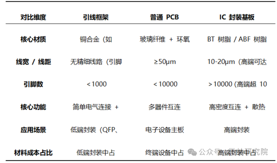
From the table, it is clear that the lead frame is a low-cost basic model suitable for low pin count scenarios; the ordinary PCB is a general-purpose model suitable for multi-device connections in end devices; while the packaging substrate is a “high-end custom model” designed for high integration chips, essential for CPU, GPU, and advanced memory chip packaging.
Understanding the Positioning of Different Substrates
The classification of packaging substrates is not arbitrary but is precisely matched to downstream demands, with clear boundaries in technical parameters and application scenarios for different types of substrates.
1. Classification by Material
This is the most critical classification method, directly determining the performance and cost of the substrate.
Rigid packaging substrates: The mainstream type, accounting for over 80%, further divided into BT resin substrates and ABF resin substrates. BT resin substrates are lower in cost, with line width/spacing of about 15-20μm, suitable for mid-to-high-end memory chips and logic chips; ABF resin substrates offer superior performance, with line width/spacing achievable below 10μm, making them the first choice for advanced packaging, such as Intel’s Xeon CPUs and TSMC’s CoWoS packaging, which both use ABF substrates.
Flexible packaging substrates: Made from PI (polyimide), characterized by flexibility and lightweight, with line width/spacing of about 20-30μm, suitable for chip packaging in wearable devices and flexible screen smartphones, adapting to the bending shapes of devices.
Ceramic packaging substrates: Made from aluminum nitride and aluminum oxide, offering good thermal conductivity and high-temperature resistance, but at a high cost and processing difficulty, mainly used in power devices and aerospace chips where heat dissipation and reliability are critically important.
2. Classification by Packaging Process
Based on the connection method between the chip and the substrate, it can be divided into two categories.
WB (Wire Bonding) substrates: The chip connects to the substrate pads via metal wires (gold or aluminum), with larger pad spacing (≥50μm), lower technical requirements, and about 30% lower cost than FC substrates, suitable for mid-to-low-end logic chip and sensor packaging.
FC (Flip Chip) substrates: The chip connects directly to the substrate pads via solder balls, with smaller pad spacing (10-20μm), requiring higher line precision and flatness, suitable for high-end chips, enabling higher interconnection density and signal transmission speed.
3. Classification by Application Field
Memory chip substrates: Mainly using BT resin substrates, requiring high stability, with line width/spacing of about 15-20μm, primarily used for DDR5 and NAND Flash packaging;
Logic chip substrates: High-end primarily using ABF substrates, requiring high pin counts and high-frequency signal transmission, used for CPUs, GPUs, and mobile SoCs;
Sensor substrates: Mostly ceramic or flexible substrates, requiring high precision and anti-interference, used for automotive sensors and industrial sensors;
Communication chip substrates: Primarily using BT or ABF substrates, requiring low-loss high-frequency signal transmission, used for 5G RF chips and optical communication chips.
Why is the Packaging Substrate a “Bottleneck” Link?
Despite the high technical barriers and significant cost share of packaging substrates, domestic companies hold less than 20% market share, with high-end ABF substrates almost monopolized by companies like Japan’s Ajinomoto and Taiwan’s Unimicron. The core reasons are threefold.
1. High Technical Barriers
The line width/spacing of packaging substrates must be below 10μm, requiring high-precision exposure and etching equipment, and domestic equipment’s precision and stability still lag behind international giants. Additionally, the formulas and production processes for core materials like ABF resin and high thermal conductivity ceramics are controlled by a few companies, making it difficult for domestic enterprises to mass-produce high-quality substrates.
2. Long Certification Cycle
Packaging substrates require dual certification from chip design and packaging factories, with a certification cycle lasting 1-2 years. Once integrated into the supply chain, customers are unlikely to easily switch suppliers, making it difficult for new entrants to break through the existing landscape.
3. High Capital Investment
The construction of production lines for packaging substrates requires substantial investment, and improving yield requires long-term process accumulation, which small and medium-sized enterprises find difficult to bear in terms of upfront investment and trial-and-error costs.