Many PCB products inevitably encounter component damage and failure after being launched. The best practice for this situation is to take preventive measures during PCB design to reduce the failure probability of fragile components during operation. Below, we will discuss which parts of the PCB are most likely to be damaged, hoping to help our friends.

If the PCB circuit board has unreasonable design, the first issue is definitely the heat dissipation problem. The majority of circuit board damage is due to poor heat dissipation design, leading to heat accumulation and significantly reducing lifespan. Secondly, the copper foil lines on the PCB board, if the width is too thin, can easily burn out due to overcurrent, causing the mainboard to malfunction. Therefore, to reduce damage failures, it is essential to ensure good heat dissipation design and reasonably increase the width of the copper foil lines.
The components and areas with high usage frequency on the PCB board are also sources of damage failures. Due to long-term use, components and areas with high usage frequency experience more severe aging compared to others. Therefore, it is necessary to implement reasonable wear protection measures, such as for drive clicks, shafts, switch tubes of power supplies, and frequently used buttons on operation panels.
Important chips and components on the PCB circuit board are equipped with protection circuits to prevent impact and other influences. When an anomaly occurs in the equipment, the first to sacrifice will inevitably be these protection circuits, which is why protection circuits are often the parts replaced during PCB repairs.
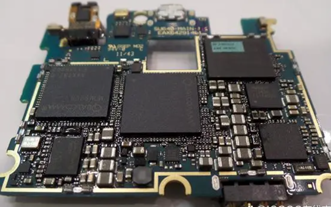
High power, heavy load, and high voltage components, such as power supplies, driver circuits, power control devices, and operational amplifiers, are generally located close to heat sinks. If protection measures and heat dissipation designs are not adequately implemented, they are likely to fail first.
For example, poor contact between the board and slot, intermittent connections inside cables, poor contact of plugs and terminals, and cold solder joints of components all fall into this category.
In addition, for more issues, you can check out the newly launched “Altium Designer Corporate Training Course”, specifically designed for companies.
This course is exclusively for PCB engineers, taught hands-on by renowned instructor Zheng Zhenyu, utilizing practical training to ensure engineers can learn without worries, significantly shortening the learning cycle and enhancing their project experience and technical level. Additionally, courses can be customized according to corporate models and development prospects to strengthen corporate competitiveness. Many new product discounts are available, hurry and grab them!


For specific inquiries, please consult the teaching assistant.
Or input “AD Corporate Training” in the public account.
▼ Scan the QR code to register or inquire ▼

Contact customer service to register immediately