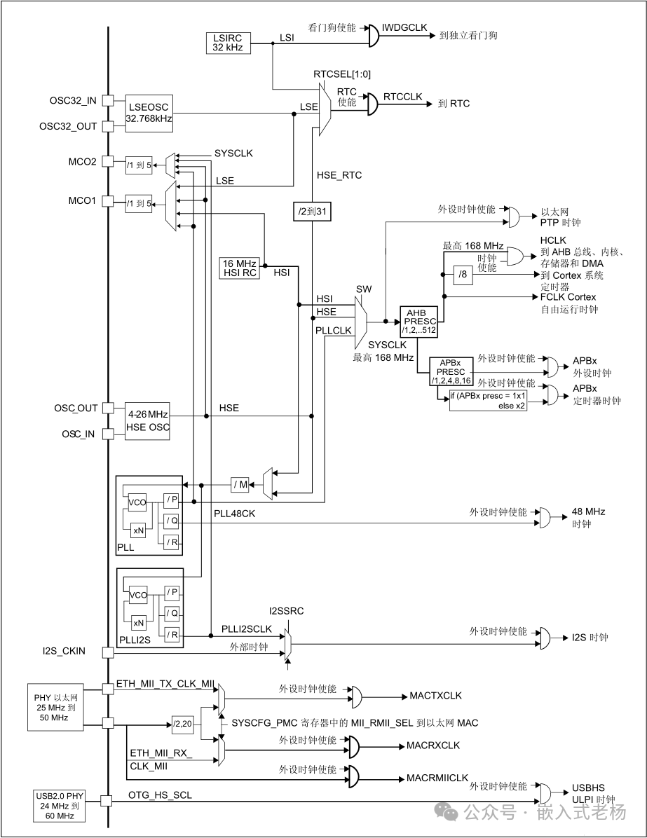
In embedded systems, the clock is the “pulse” of the microcontroller (MCU) — every data transfer, instruction execution, and peripheral operation relies on the precise synchronization of clock signals. The “clock tree” is an intelligent system that manages these “pulses”; it resembles a large tree with distinct branches, starting from the root of the original clock source, through the trunk (phase-locked loop) and branches (buses), delivering the appropriate clock frequency to each “leaf” (peripheral). For high-performance MCUs like the STM32F407, the design of the clock tree directly determines the system’s performance ceiling, peripheral compatibility, and power consumption levels. This article will use the STM32F407 as an example, combining HAL library instances to explain the core role of the clock tree in simple terms.
01
—
The “Timing Commander” of Embedded Systems
Imagine a busy port: container cranes need to operate at high speed (corresponding to high-frequency peripherals), while the gatekeeper’s access control system only needs to work at low speed (corresponding to low-frequency peripherals). All devices must collaborate based on a unified time reference, while idle devices should power down to save energy. The clock tree is such a “commander”:
Providing a reference timing: The speed at which the CPU executes instructions, the rhythm of serial port data transmission, and the precision of timer counting are all based on clock signals. Without a clock, hardware is like a “disoriented band”, unable to perform any orderly operations.
Adapting to diverse needs: Different peripherals have vastly different requirements for clock frequency. For example, GPIO level toggling only requires a few MHz, SPI communication may need 84MHz, while high-precision ADCs may even require 168MHz. The clock tree can “customize” frequencies for each peripheral through division and multiplication mechanisms.
Optimizing system power consumption: The peripheral clocks of the STM32F407 are turned off by default (similar to “standby mode”) and are only activated when in use. This “on-demand power supply” design can significantly enhance the battery life of powered devices.
The clock tree design of the STM32F407 is a “precision instrument” that can generate a system clock of up to 168MHz from the original clock source while allocating precise frequencies to dozens of peripherals, making it the “unsung hero” of stable system operation.
02
—
The “Branching Structure” of the STM32F407 Clock Tree
The clock tree of the STM32F407 resembles a layered tree, and we will analyze it layer by layer from the “roots” to the “leaves”:
1. Clock Sources
The clock source is the starting point of the clock tree, providing the most basic clock signals. The STM32F407 has four core “roots”, akin to different precision “original generators”:
HSI (High-Speed Internal Clock): An integrated 16MHz oscillator within the chip. It requires no external components and can start up immediately, but has lower accuracy (error of about ±1%), suitable for quick testing or simple scenarios without an external crystal.
HSE (High-Speed External Clock): Provided by an external crystal (commonly 8MHz or 16MHz), with extremely high accuracy (error within ±0.1%). It is the preferred main clock for the system, especially suitable for timing-sensitive scenarios (such as high-speed communication and precise timing).
LSI (Low-Speed Internal Clock): A 32kHz internal oscillator with lower accuracy, mainly providing a backup clock for low-power timers (such as SysTick) and RTC (real-time clock).
LSE (Low-Speed External Clock): A 32.768kHz external crystal (matching the frequency of watch crystals), specifically designed for RTC to ensure the accuracy of calendar and alarm functions.
These clock sources do not operate simultaneously; the system selects one as the “main power source” based on demand, which is then processed by subsequent circuits and distributed to various modules.
2. Phase-Locked Loop (PLL)
The frequency of the original clock source often cannot meet high-performance requirements (for example, HSE is usually 8MHz, while the CPU needs 168MHz). The role of the phase-locked loop (PLL) is to “amplify” the low-frequency clock to high frequency, acting as a “clock amplifier”.
The STM32F407 includes two core PLLs:
Main PLL: The system’s “main amplifier”, with input clocks coming from HSI or HSE, generating high-frequency clocks through three levels of processing:
Division (PLL_M): Divides the input clock (range 2-63), for example, an 8MHz HSE divided by PLL_M=8 results in 1MHz.
Multiplication (PLL_N): Multiplies the divided clock (range 64-432), for example, 1MHz multiplied by PLL_N=336 results in 336MHz.
Division (PLL_P): Divides the multiplied clock (optional 2, 4, 6, 8), with the final output serving as the system main clock (SYSCLK). For example, 336MHz divided by PLL_P=2 results in 168MHz (the maximum system clock for F407).
PLLI2S: A “dedicated amplifier” designed for I2S audio peripherals, capable of generating high-precision clocks (audio is sensitive to clock jitter), ensuring that audio sampling rates are accurate.
3. Bus Clock Distribution
The system main clock (SYSCLK) is distributed to different buses through “distribution pipelines” (dividers), which then provide clocks to peripherals. The buses of the STM32F407 are like different speed-limited “highways”:
AHB Bus (HCLK): The “main road”, connecting the CPU, memory, DMA, and other core modules. It is derived from SYSCLK through the AHB prescaler (1-512 division), with a maximum of 168MHz (when the prescaler = 1).
APB1 Bus (PCLK1): The “low-speed lane”, connecting low-speed peripherals (such as USART2, I2C1, TIM2). It has a maximum of 42MHz (when SYSCLK=168MHz, the prescaler = 4, 168/4=42MHz).
APB2 Bus (PCLK2): The “high-speed lane”, connecting high-speed peripherals (such as USART1, SPI1, TIM1, GPIO). It has a maximum of 84MHz (when SYSCLK=168MHz, the prescaler = 2, 168/2=84MHz).
These buses not only transmit data but also determine the base clock frequency for the peripherals connected to them.
4. Peripheral Clock Enable
The peripheral clocks of the STM32F407 are turned off by default (similar to “device power off”); they must be manually enabled when in use — this is a detail that beginners often overlook. For example:
GPIOA is connected to the AHB1 bus and requires __HAL_RCC_GPIOA_CLK_ENABLE() to enable the clock;
USART1 is connected to the APB2 bus and requires __HAL_RCC_USART1_CLK_ENABLE() to enable the clock.
If the clock is not enabled, even if the code logic is correct, the peripheral will be “unresponsive” (register read/write will be ineffective).
03
—
Example: How Does the Clock Tree “Command” Peripheral Operations?
The role of the clock tree is not an abstract concept; it directly determines whether peripherals can function properly. The following three common scenarios intuitively demonstrate the “command logic” of the clock tree:
Example 1: LED Blinking — The Clock Dependency of GPIO and SysTick
The core of LED blinking is “GPIO level toggling” + “delay waiting”, both of which depend on the precise control of the clock tree.
Clock source for GPIO:
GPIOA is connected to the AHB1 bus, and its clock is provided by HCLK. Assume the system configuration is: HSE=8MHz → Main PLL outputs 168MHz (SYSCLK=168MHz) → AHB prescaler = 1 (HCLK=168MHz) → AHB1 peripheral clock = 168MHz.
To control the PA5 pin (connected to the LED), the GPIOA clock must first be enabled:
// HAL library code: Enable GPIOA clock__HAL_RCC_GPIOA_CLK_ENABLE();// Configure PA5 as output modeGPIO_InitTypeDef GPIO_InitStruct = {0};GPIO_InitStruct.Pin = GPIO_PIN_5;GPIO_InitStruct.Mode = GPIO_MODE_OUTPUT_PP;GPIO_InitStruct.Pull = GPIO_NOPULL;GPIO_InitStruct.Speed = GPIO_SPEED_FREQ_VERY_HIGH;HAL_GPIO_Init(GPIOA, &GPIO_InitStruct);
If the clock is not enabled, HAL_GPIO_Init() will fail, and PA5 will remain at its default level (LED will not light up).
Clock source for delay:
The delay function relies on the SysTick timer (built into the Cortex-M4 core), whose clock source can be configured as HCLK (168MHz) or HCLK/8 (21MHz). For example, if configured as HCLK=168MHz, SysTick counts 168 times to represent 1μs, achieving a 100ms delay through HAL_Delay(100):
// Toggle LED and delay 100msHAL_GPIO_TogglePin(GPIOA, GPIO_PIN_5);HAL_Delay(100); // Relies on SysTick clock
If the SysTick clock is configured incorrectly (e.g., mistakenly set to HCLK/8), the 100ms delay will actually become 800ms, causing the LED to blink noticeably slower.
Example 2: Serial Communication — The Relationship Between Baud Rate and USART Clock
The core of serial communication is the “baud rate” (e.g., 115200 bit/s), and its accuracy is entirely determined by the clock. USART1 is connected to the APB2 bus, and its clock frequency = PCLK2 (84MHz, when the APB2 prescaler = 2).
The STM32F407’s USART employs a flexible division mechanism, with the baud rate calculation formula as follows:
USARTDIV = USART clock frequency / Baud rate
Where USARTDIV includes both integer and fractional parts (to ensure high precision). For example, the calculation of the baud rate 115200:
USARTDIV = 84,000,000 / 115,200 ≈ 729.1667
The HAL library will automatically calculate and configure the USART’s BRR register:
// HAL library code: Configure USART1 baud rate to 115200UART_HandleTypeDef huart1;huart1.Instance = USART1;huart1.Init.BaudRate = 115200;huart1.Init.WordLength = UART_WORDLENGTH_8B;huart1.Init.StopBits = UART_STOPBITS_1;huart1.Init.Parity = UART_PARITY_NONE;huart1.Init.Mode = UART_MODE_TX_RX;huart1.Init.HwFlowCtl = UART_HWCONTROL_NONE;HAL_UART_Init(&huart1); // Internal automatic division calculation
If the APB2 clock is incorrect (e.g., actually 42MHz), the actual baud rate will become 57600, leading to garbled serial communication (the receiver cannot recognize the signal).
Example 3: Timer Timing — The Clock Multiplication Mechanism of TIM1
Timers (such as TIM1) are used for precise timing (e.g., PWM output), and their clock frequency is affected by the APB2 prescaler, with the rules as follows:
If the APB2 prescaler = 1 (PCLK2=HCLK), then TIM1 clock = PCLK2;
If the APB2 prescaler > 1 (e.g., 2), then TIM1 clock = 2×PCLK2 (multiplication mechanism, ensuring high-speed counting).
Assuming the system configuration is HCLK=168MHz, APB2 prescaler = 2 (PCLK2=84MHz), then TIM1 clock = 2×84MHz=168MHz. To generate a 1ms timing (counting 168,000 times):
// HAL library code: Configure TIM1 to time 1msTIM_HandleTypeDef htim1;htim1.Instance = TIM1;htim1.Init.Prescaler = 0; // No divisionhtim1.Init.CounterMode = TIM_COUNTERMODE_UP;htim1.Init.Period = 167999; // Count from 0 to 167999 for a total of 168000 timeshtim1.Init.ClockDivision = TIM_CLOCKDIVISION_DIV1;HAL_TIM_Base_Init(&htim1);
If the multiplication mechanism is not understood (mistakenly treating TIM1 clock as 84MHz), then the 1ms timing will actually become 2ms, leading to incorrect PWM duty cycle (e.g., expected 50% but actually 25%).
04
—
Conclusion
The clock tree of the STM32F407 may seem complex, but it is actually a balance of “precision” and “flexibility”:
Timing reference: Without the clock tree, the CPU cannot execute instructions, and peripherals cannot work together — the clock is the “lifeline” of embedded systems.
On-demand allocation: Through PLL and dividers, high-frequency rates are provided for high-speed peripherals and low-frequency rates for low-speed peripherals, avoiding “performance waste”.
Power consumption optimization: Peripheral clocks are “turned on demand”, significantly reducing idle power consumption, which is crucial for battery-powered devices.
For developers, the key to understanding the clock tree is that the first step in using any peripheral is to confirm its clock source and correctly configure the frequency. Utilizing the STM32CubeMX tool (which visually configures the clock tree and automatically generates HAL library code) can greatly reduce the difficulty of manual configuration, allowing us to focus more on functional implementation rather than timing details.
Previous Articles:
AI Smart Rings: Small Size, Big Technological Energy
Detailed Explanation of Motor Principles and Classifications
Introduction to Peripheral Component Selection and Layout for Switching Power Supplies (DCDC)
Bare Metal Programming and RTOS Programming
Development Board “Battle Royale”: Which of the 5 Popular Development Boards from FeiLing, YouShan, TianMai, etc. is Your “Dish”?
Calculating FreeRTOS Task Stack Size
5 Major State Machine Design Patterns in Embedded Systems
The Difference Between MCU and MPU
In-Depth Analysis of AMD Ryzen Embedded 8000 Series Processors
Usage of the “volatile” Keyword in Embedded C Language