As manufacturers begin to release high-performance MCUs, it is becoming increasingly difficult to distinguish between MCUs and MPUs.
Back in 2022, when Arm launched the Cortex-M85, an engineer remarked, “Although the M85 is a Cortex-M, I believe its performance has surpassed that of early Cortex-As. The upcoming M85 processors are not just microcontrollers; they can be considered micro-application processors.”
Recently, manufacturers have started to invest more in M85 MCUs, and these products seem to truly possess capabilities that rival those of MPUs. What are the highlights of these products? EEWorld will summarize them today.

Understanding the M85’s Inner Workings
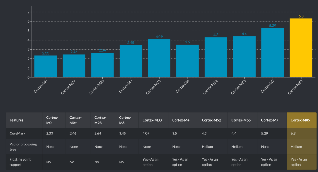
Performance is one of the most straightforward advantages of the M85.
The M85 is the first Cortex-M to support over 6 CoreMarks/MHz and more than 3 DMIPS/MHz. Additionally, through Arm Helium technology, the M85 achieves a fourfold increase in DSP and ML processing compared to its predecessor, the M7. This level of scalar performance is attributed to numerous innovative features at the microarchitecture level, including optimized dual-issue and selective triple-issue capabilities, improved branch prediction, and an enhanced memory system that includes data prefetching.
According to Arm, in the face of increasingly demanding computational requirements, developers of Cortex-M microcontroller systems face a dilemma: whether to optimize software to extract more clock cycle processing power from existing microcontrollers or to migrate codebases to higher-performance microprocessor architectures. Cortex-M microcontrollers offer multiple advantages, including deterministic execution, short interrupt latency, and advanced low-power management modes. Transitioning to Cortex-A processors means sacrificing some of the inherent advantages of Cortex-M. Therefore, the Cortex-M line must introduce a product with such explosive performance.
In simple terms, it aims to satisfy the desire for both high performance comparable to MPUs and the low BOM cost control, low power consumption, and ease of development characteristic of MCUs.
The memory system architecture is another advantage of the M85.
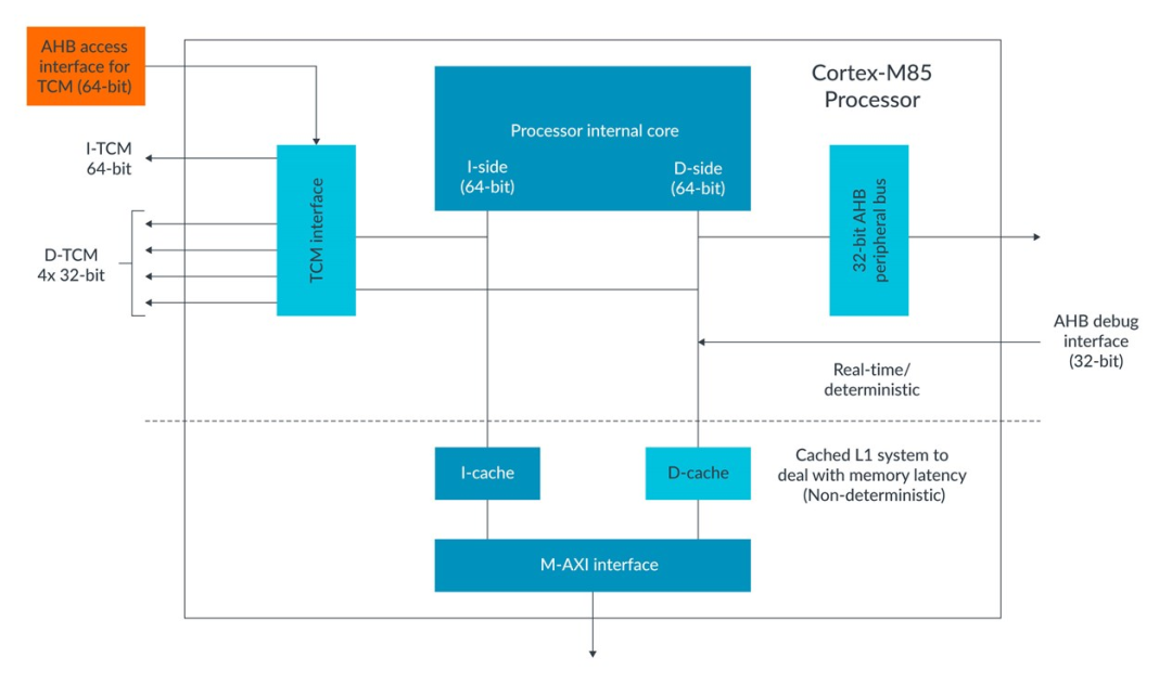
The M85 features a low-latency memory system with tightly coupled memory (TCM) that ensures deterministic operation. This architecture provides SoC designers with four 32-bit data TCM interfaces and one 64-bit instruction TCM interface, all of which integrate error correction code (ECC) functionality. The new 32-bit AHB access interface port allows external DMA controllers to concurrently access the M85 processor core’s TCM, supporting various common data stream processing application scenarios.
Scan the code and send the secret code: MCU, to join the relevant technical exchange group

The M85 memory system also includes a level 1 cache system equipped with ECC, connected to external memory via the AMBA 5 AXI master interface, maintaining performance optimization even in the face of low-speed, non-deterministic memory access.
Security is another major selling point of the M85.
The M85 introduces the TrustZone technology from the Armv8-M architecture and becomes the first Cortex-M processor to integrate the Armv8.1-M pointer authentication and branch target identification extension (PACBTI), significantly lowering the implementation threshold for developers to achieve PSA security certification level 2.
PACBTI provides enhanced protection against return-oriented and jump-oriented software attacks by verifying function calls and return addresses.
In summary, the unprecedented performance level brought by the M85 opens up new horizons for MCU developers, and manufacturers have expressed their readiness to follow suit. However, updates and iterations do not happen overnight, and how the M85 is positioned will also be a question. Now, it seems that the time for the M85 to shine has come.

ST Takes ActionST recently launched the STM32V8, sparking discussions among many users on EEWorld. This product is one of the highest-performing in the STM32 series of microprocessors, achieving a terrifying EEMBC CoreMark score of 5072, significantly higher than that of the STM32N6.
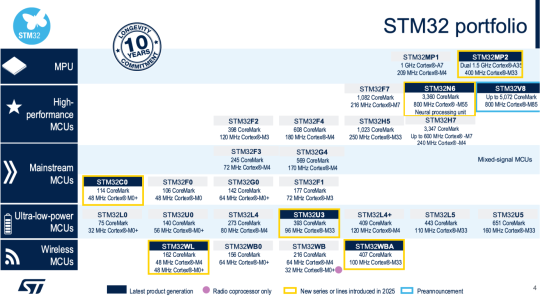
18nm, 800MHz Cortex-M85, 4MB PCM (phase change memory), MVE (Arm Helium M-profile Vector Extension) — these keywords all reflect the strength of this product.
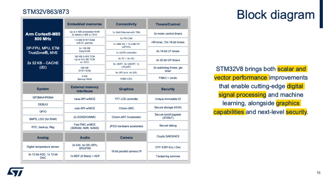
According to ST, simply upgrading to the M85 core improves scalar mathematical operation performance in real-time control applications by 20%; compared to Cortex-M7 products, performance increases by 3.5 times at the same clock frequency; applications relying on DSP functionality see performance increases of up to 300%~400%.
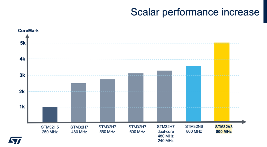
The ability to achieve such powerful performance is closely related to its use of the 18nm FD-SOI PCM process, which is the same as that used in the automotive MCU Stellar series. FD-SOI forms a competitive landscape with FinFET, which also provides high-performance computing. This technology is relatively new in the MCU field, enabling the STM32V8 to achieve higher operating speeds while significantly optimizing power efficiency.
PCM is an embedded non-volatile memory (NVM) technology that has developed various forms, including Intel’s discontinued 3D XPoint memory, known for its speed. Due to the limitations of embedded flash (eFlash) technology, MCUs have been stuck at the 40nm process node. To shrink the process, the industry is focusing on new types of storage.
PCM is a storage technology that competes with MRAM, FRAM, and RRAM. PCM offers the smallest storage units in its class, allowing for more than double the information storage capacity in the same area, providing physical advantages and achieving the smallest storage area. It can double the overall storage capacity without increasing costs, undoubtedly leading to further cost reductions.
More importantly, compared to MRAM and FRAM, ST’s PCM has additional advantages: it supports a maximum operating temperature of 140°C, and its radiation resistance makes it suitable for aerospace applications as well as meeting the stringent demands of industrial and automotive applications. Thus, we see that one of the major applications of the STM32V8 is in aerospace.
This series of chips supports up to 4MB of ePCM and 1.5MB RAM, with external serial memory interfaces including eight-line SPI (8-bit) and sixteen-line SPI (16-bit), supporting serial NOR flash, HyperRAM, PSRAM, and execute-in-place (XIP) operations.
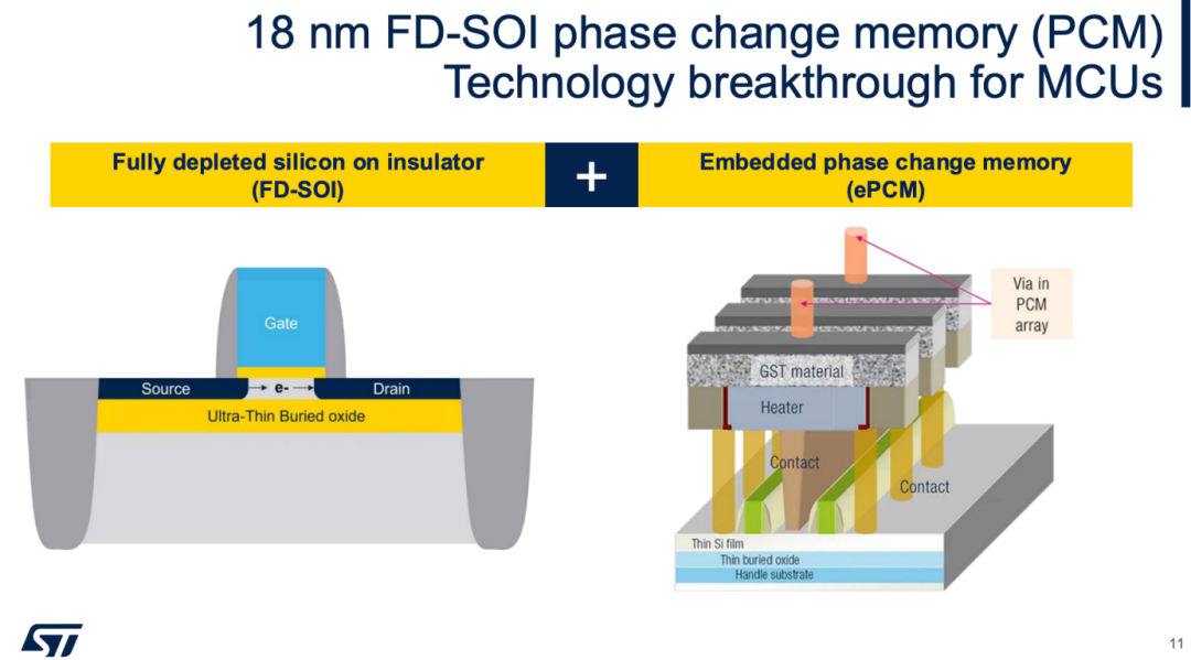
The significant enhancement of AI capabilities is another advantage of the STM32V8.
Through the Arm Helium M-profile vector extension (MVE) technology, it builds the foundation for AI capabilities. Helium, based on single instruction multiple data (SIMD) and single-element scalar instructions, supports both integer and floating-point operations, covering 8-bit to 64-bit integer operations and 128-bit vector operations with 16/32-bit floating-point calculations. This technology brings enhanced machine learning (ML) and digital signal processing (DSP) capabilities to high-performance microcontrollers, and Arm has packaged MVE into function libraries and code generation tools suitable for C/C++ development.
Along with the product launch, ST has also upgraded its edge AI product line with an AI model library. This library gathers pre-trained AI models covering various AI application scenarios. These models are optimized for ST’s AI microcontroller product portfolio, accelerating the edge AI development process. According to official information, the model library currently contains over 140 models, applicable to wearable devices, smart cameras and sensors, security devices, and robots, providing visual, audio, and perception capabilities.
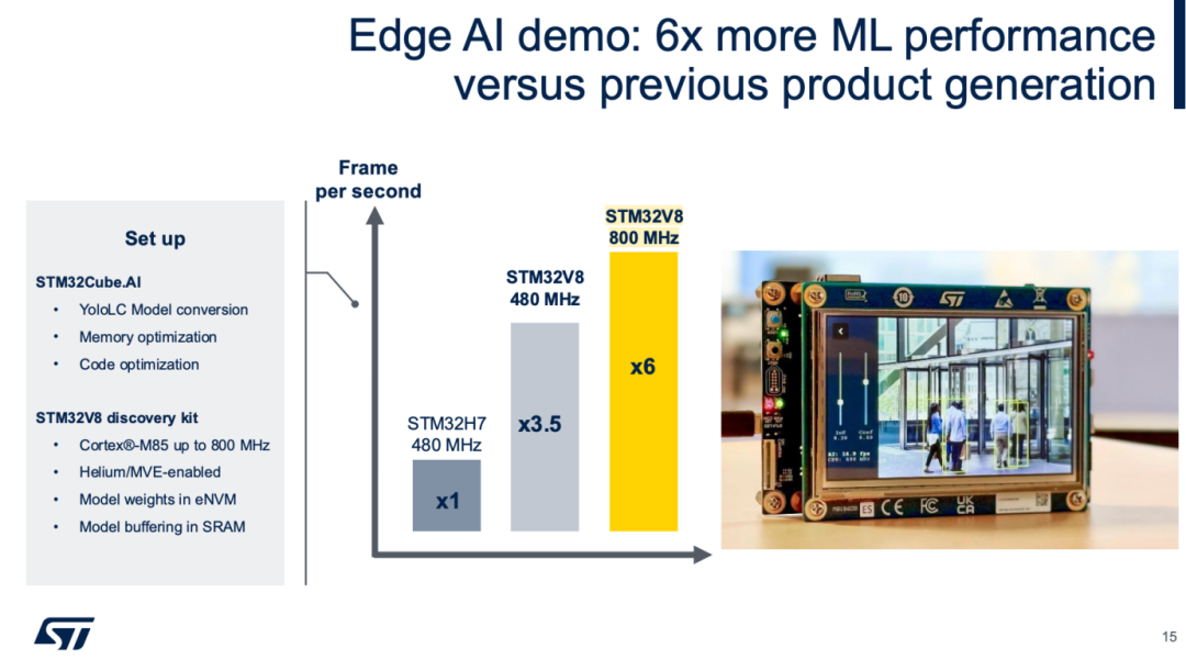
The STM32V8 also has other minor upgrades, including: an integrated Chrom-ART graphics accelerator, TFT LCD controller, and JPEG accelerator; a gigabit Ethernet controller supporting time-sensitive networking (TSN), along with interfaces such as FD-CAN, high-speed USB, and HDMI-CEC; including 12-bit ADC and DAC interfaces, as well as two sets of SAI and four sets of I2S audio interfaces; covering secure storage, secure boot, and secure debugging support; equipped with unique identity and anti-tampering mechanisms, and certified by PSA Level 3 and SESIP 3 security standards.

Renesas’ Early Layout
Renesas has been laying out the M85 for a longer time, and its updated products are also exceptionally diligent and frequent.
In October 2023, Renesas launched the industry’s first MCU based on the Arm Cortex-M85 processor, the RA8 series — RA8M1, achieving a groundbreaking 3000 CoreMark, meeting the requirements for complete determinism, low latency, and real-time operation. According to Renesas, the performance level of 6.39 CoreMark/MHz will enable system designers to replace commonly used MPUs with the RA MCU.
At that time, Renesas’ first-generation RA8 mainly expanded the product line around the M85 core, featuring a 480MHz M85 with Helium MVE, and did not introduce new types of storage, equipped with 1MB~2MB flash and 1MB SRAM (including TCM).
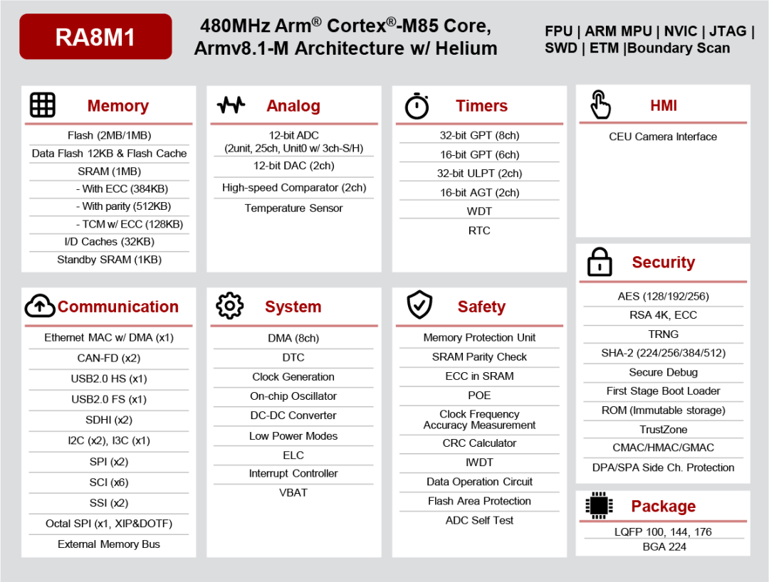
This June, Renesas quietly launched the “World’s Strongest MCU” RA8P1 series on its official website.
The second generation of the RA8 has upgraded the process to 22nm ULL technology, equipped with new storage options of 0.5/1MB MRAM (optional 4/8MB flash), and the main frequency has also significantly increased, reaching 1GHz for the M85 core, compared to the RT1170 which uses a 28nm FD-SOI process technology.
According to Renesas, compared to flash memory, MRAM offers faster write speeds, higher durability, and stronger data retention capabilities. Moreover, to pursue better AI performance, the second generation of the RA8 also integrates the Ethos-U55 NPU and another 250MHz M33.
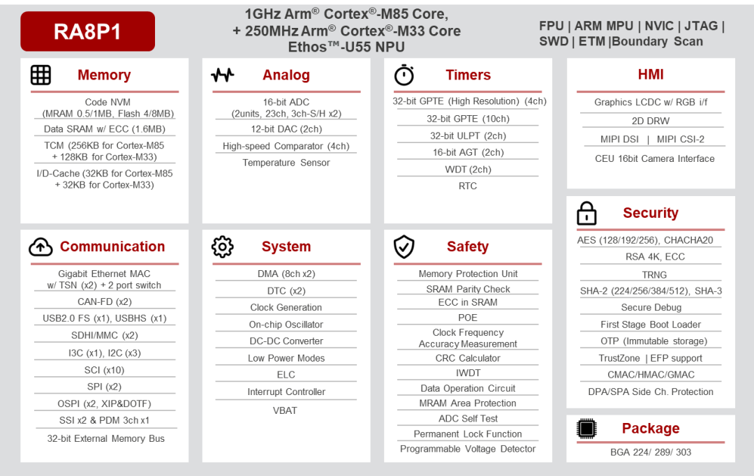
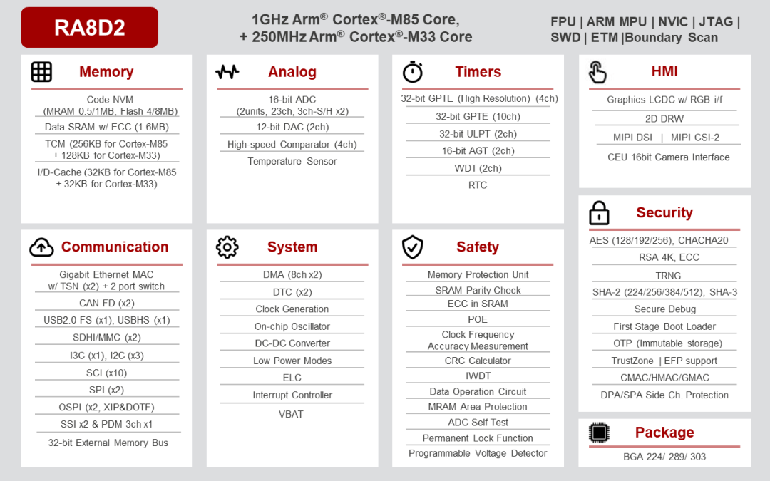
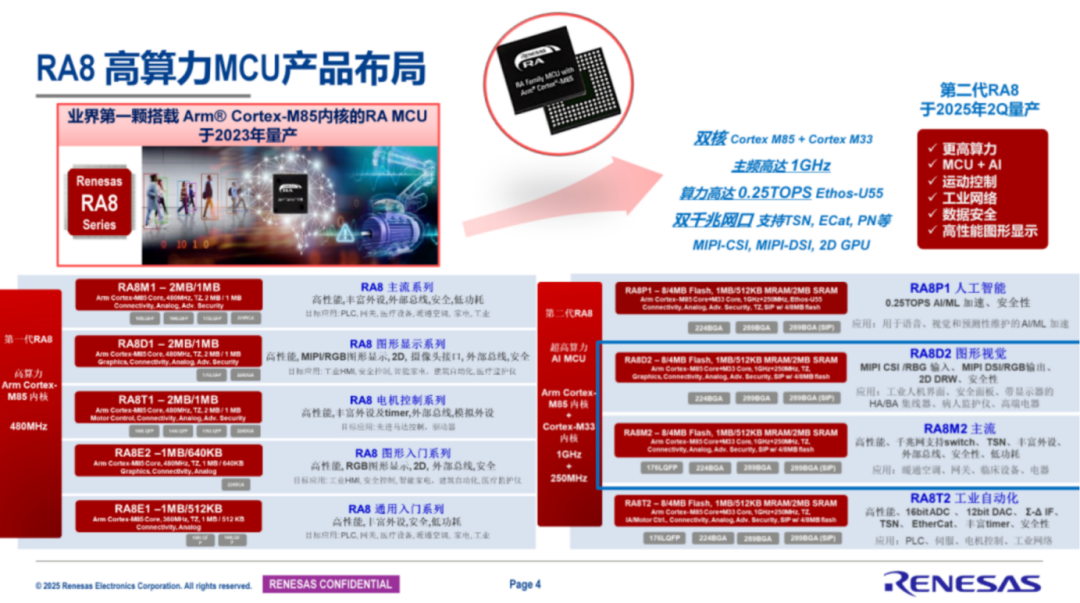
With the launch of RA8P1, Renesas also introduced the RA8D2, which is also equipped with the 1GHz M85 core and new storage MRAM.
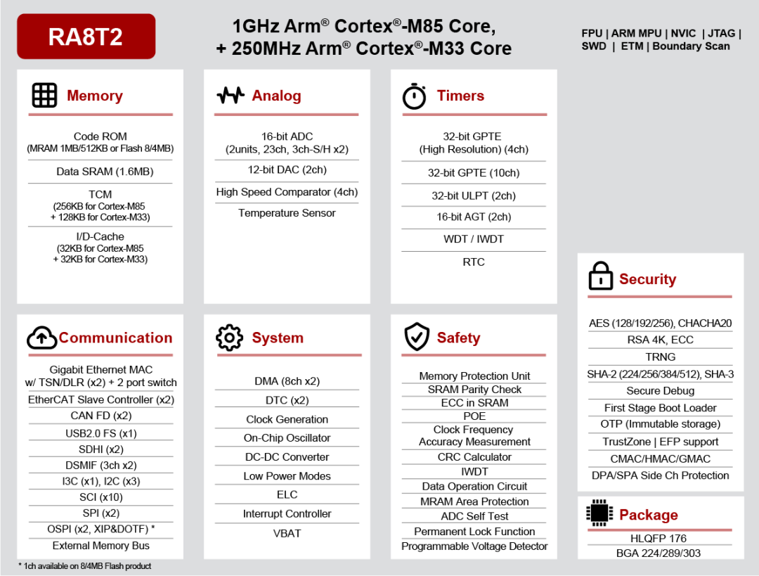
This October, Renesas continued to iterate, launching the 1GHz RA8T2 Cortex-M85 microcontroller, integrating MRAM and EtherCAT to empower industrial motor control microcontrollers. This product integrates 1MB MRAM, 2MB with ECC verification SRAM, while providing dual cores with 256KB (M85) and 128KB (M33) tightly coupled memory (TCM), and supports SiP packaging expanded to 8MB of external flash.
Shortly after, Renesas added two new products to the RA8 series, RA8M2 and RA8D2, and refreshed the benchmark, achieving a terrifying 7300 CoreMark.
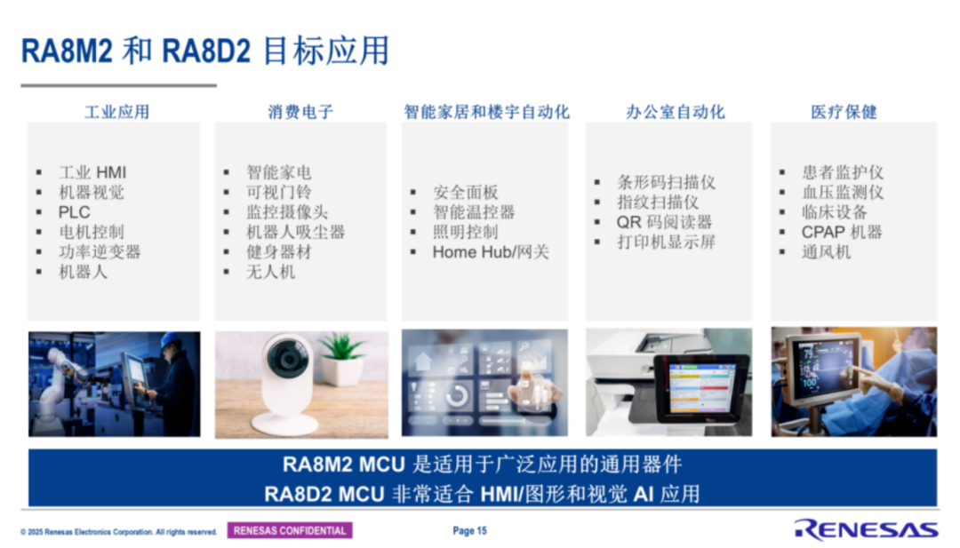
Renesas states that the RA8M2 and RA8D2 are equipped with embedded MRAM, which has multiple advantages over flash memory technology — high durability, stronger data retention capabilities, faster write speeds, no erase operations required, byte-addressable, and lower leakage current and manufacturing costs. For higher-demand applications, SIP options with 4 or 8MB of external flash are also available. Additionally, both RA8M2 and RA8D2 MCUs include gigabit Ethernet interfaces and dual-port TSN switches to meet the needs of industrial network applications.
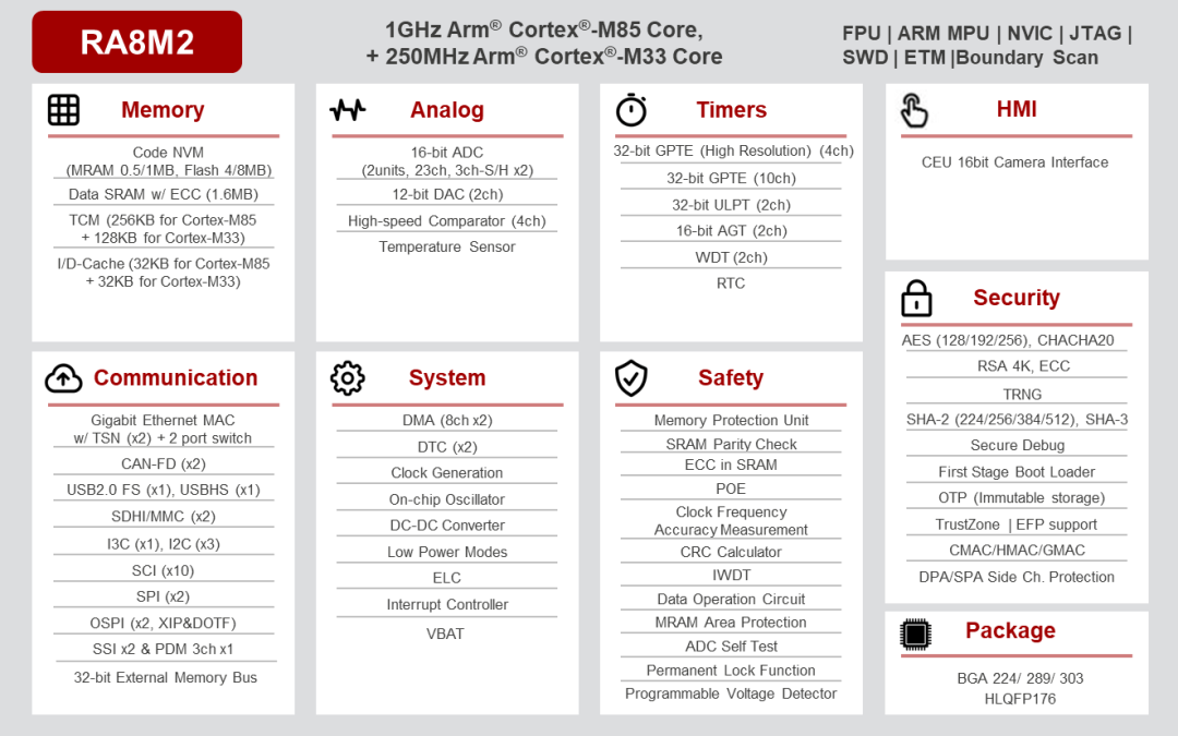
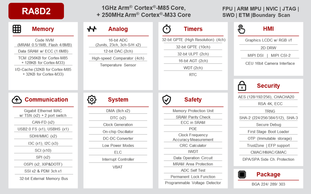
It can be said that Renesas has recently been focusing on high-performance MCUs, and in order to achieve higher process technology and stronger performance, it has also been focusing on MRAM.

Final Thoughts
With the introduction of the M85 into the MCU space, we are truly struggling to distinguish between MCUs and MPUs. Clearly, these layouts are aimed at AI, which is indeed providing significant momentum for product upgrades.
The M85 is redefining the boundaries of high-performance embedded systems with its performance that surpasses traditional MCUs and heterogeneous integration capabilities, leading MCUs into a new era of “unbounded computing power“.
References
[1]Arm:https://developer.arm.com/community/arm-community-blogs/b/internet-of-things-blog/posts/introducing-cortex-m85
[2]All About Circuits:https://www.allaboutcircuits.com/news/stmicro-unveils-first-18-nm-mcu-for-high-performance-designs/
[3]Electronic Design:https://www.electronicdesign.com/technologies/embedded/article/55332065/electronic-design-stmicroelectronics-stm32v8-utilizes-fd-soi-and-phase-change-memory
[4]ST:https://www.st.com/resource/en/product_presentation/stm32v8-presentation.pdf
[5]Renasas:https://www.renesas.cn/
· END ·
Welcome to follow the subscription account of EEWorld: "Robot Development Circle"
Scan the code to add the assistant and reply “robot”
to join the group and exchange experiences face-to-face with electronic engineers.