In PCB (Printed Circuit Board) design, factors such as signal transmission stability and impedance matching are typically considered. Choosing the appropriate stacking scheme is crucial to meet design requirements. In certain cases, especially when designing six-layer boards, a special design scheme known as ‘pseudo eight-layer’ may be adopted.
The ‘pseudo eight-layer’ actually refers to a six-layer PCB design that, through specific layout and material selection, possesses characteristics similar to an eight-layer board. Generally, the structure of a six-layer board includes two core layers (or inner layers), two surface layers (top and bottom), and two inner layers. The ‘pseudo eight-layer’ design adds additional material layers within the six-layer board, making the overall layout closer to that of an eight-layer board.
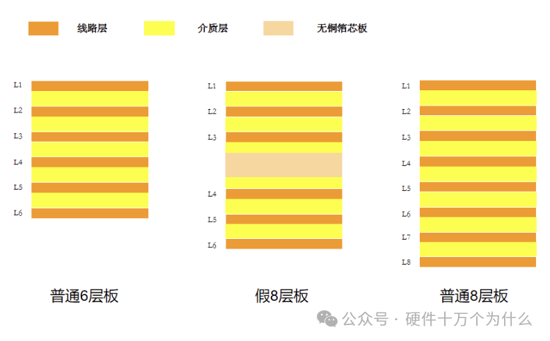
Six-Layer Board:
Eight-Layer Board:
Pseudo Eight-Layer:
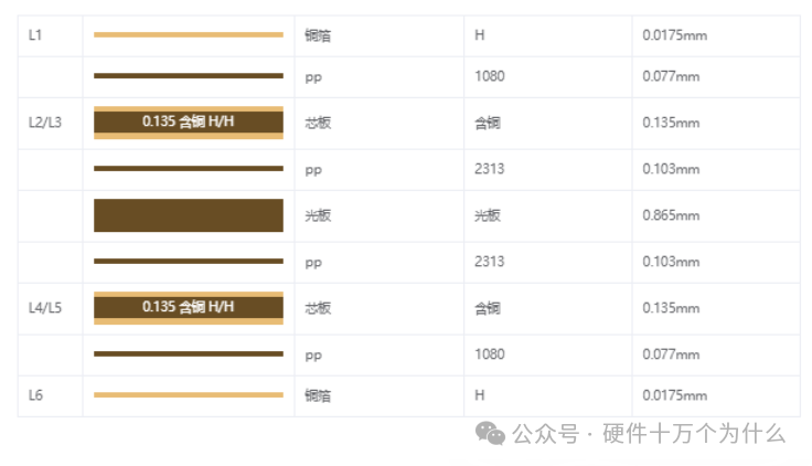
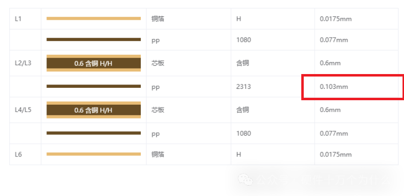
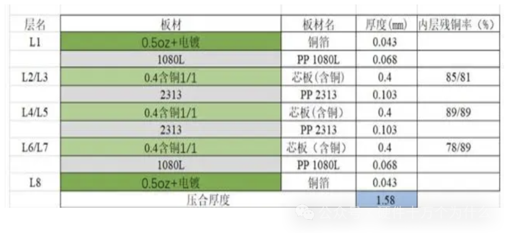
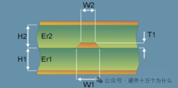
Typically, a PCB is composed of core layers, copper foil, prepreg (also known as PP), and solder mask. The core layer is the fundamental material for making PCBs, consisting of copper foil, solid resin material, and fiberglass. The prepreg is made of resin and reinforcement materials, with fiberglass cloth being the most commonly used reinforcement material.
Core Layer: Made of copper foil, solid resin material, and fiberglass, it serves as the fundamental material for PCB production, possessing certain hardness and thickness, with copper foil on both surface layers.
Copper-Free Core Layer: A core layer without copper foil on both surface layers.
Prepreg (PP): Mainly composed of resin and reinforcement materials, which can be categorized into fiberglass cloth, paper-based, composite materials, etc. The prepreg used for multilayer printed boards is mostly made with fiberglass cloth as the reinforcement material.
In cases where impedance is required, adopting the pseudo eight-layer design can reduce our design line width, thus meeting our design requirements. When routing on the third and fourth layers of a six-layer board, using the pseudo eight-layer design can reduce crosstalk between the third and fourth layers, as they are adjacent layers. If both layers are routed too closely, crosstalk can occur, affecting signal quality. Therefore, the pseudo eight-layer design increases the distance between these two layers, resulting in relatively lower crosstalk. However, we also need to pay attention to the adjacent routing layers, where we should use ‘perpendicular routing’, meaning one layer routes horizontally while the other routes vertically. Additionally, the pseudo eight-layer design must consider the reference plane issue. The impedance of a microstrip line is related to the distance and width of the planes on either side.
The pseudo eight-layer design requires complete reference planes for L3 and L4. We cannot neglect the reference plane just because we are using a pseudo eight-layer design.
Since we can increase the number of PP sheets to achieve thickness, why not use multiple PP sheets to thicken and realize a six-layer board instead of making a pseudo eight-layer? Because we cannot keep increasing the number of PP sheets; generally, we can only use up to three sheets. If too many sheets are used, there is a risk of slippage during the board pressing process. The pseudo eight-layer design achieves this by adding inner layer materials within the six-layer board. These inner layer materials are typically located between the core layers, with some materials not containing copper foil. This design can meet impedance requirements while reducing line width and minimizing crosstalk between adjacent layers, thereby improving signal quality.
So why not just use eight layers?Because the pseudo eight-layer is cheaper than the eight-layer. When produced in large quantities, cost savings are essential.
[1]Interest-Driven Passion
[2] Should Hardware Engineers Design Their Own PCBs?
[3]How Long Should PCB Traces Be??
[4]How Wide Should PCB Traces Be?
[5]Inner Layers of PCB
[6]Via
[7]Can PCB Traces Have Sharp Angles and Right Angles?
[8] Should Dead Copper Be Retained? (PCB Islands)
[9]Can Vias Be Placed on Pads??
[10] PCB Materials,What Does FR4 Refer To?
[11] Solder Mask,Why Is Green Oil Mostly Green?
[12]Steel Mesh
[13]Pre-layout
[14]Principles of PCB Layout and Routing
[15] Cross-Division Routing
[16] Signal Reflection
[17] Dirty Signals
[18] Surface Treatment Processes Such as Gold Plating, Gold Coating, and Tin Spraying
[19] Line Spacing
[20] Placement of Capacitors
[21] Crosstalk
[22] Flying Probe Testing of PCBs
[23] Overview and Simulation of FPC
[24] Why Do PCBs Deform and Bend? How to Solve It?
[25] Understanding ‘Characteristic Impedance’ in One Article
[26] PCB Stacking Design
[27] High-Speed Circuit PCB Reflow Path
[28] Power Handling and Plane Segmentation in PCB Design
[29] Zigzag PCB Routing – Tabbed Routing
[30] What Is the Dielectric Loss Angle of PCB?
[31] The Impact of PCB Copper Foil Roughness on High-Speed Signals
[32] Why Should Crystals Not Be Placed at the Edge of a PCB?
[33] What Are High-Speed Signals?
[34] What Is a Transmission Line?
[35] Pre-emphasis, De-emphasis, and Equalization
[36] How to Utilize PCB Heat Dissipation
[37] ‘Stub’ in PCB Design
[38] Dilemma: Should There Be GND Protection Traces Between Routing?
[39] PCB Copper Pour
[40] Rules to Follow When Designing PCBs
Hard Ten Published Books


‘DCDC Power Supply Chapter’ is currently in the publishing process, expected to be released in May, stay tuned.