
Source: Chip Discussion
Introduction: Since the birth of integrated circuit (chip) technology in 1958, it has a development history of 63 years. In today’s information society, chips are undoubtedly the most important foundational support. In recent years, core chip technology has become a tool for the United States to maintain technological hegemony and suppress other countries. People are eager to know how chip technology has evolved from its primitive and immature beginnings to become the technological gem of today’s high-tech crown. This article will primarily use photos and illustrations, supplemented by text, to discuss the development history of chip technology over the past 60 years. Due to space constraints, it will be divided into three parts: the first, second, and third.
To introduce the history of chip technology, we must start with the discovery and research of semiconductors, the invention of vacuum tubes, transistors, and integrated circuits. It is these discoveries, research, and inventions that have given birth to electronic technology and the electronics industry, marking the beginning of an electronic information society.
1.Discovery and Research of Semiconductors (1833-1947, 114 years)
In 1833, British scientist Michael Faraday discovered a peculiar phenomenon while testing the properties of silver sulfide (Ag2S), where the resistance of silver sulfide decreases as temperature increases, known as the resistive effect. This was the first characteristic of semiconductors discovered by humanity.
In 1839, French scientist Edmond Becquerel discovered that a junction formed by a semiconductor and an electrolyte generates a voltage under illumination, known as the photovoltaic effect, which is the second characteristic of semiconductors.
In 1873, British scientist Willoughby Smith discovered the photoconductive effect of selenium (Se) crystal materials, where conductivity increases under light, marking the third characteristic of semiconductors.
In 1874, German physicist Ferdinand Braun observed that the conductivity of certain sulfides depends on the direction of the applied electric field. When a forward voltage is applied, it conducts; when the voltage polarity is reversed, it does not conduct, which is known as the rectifying effect, the fourth characteristic of semiconductors. That same year, British physicist Arthur Schuster, born in Germany, discovered the rectifying effect of copper (Cu) and copper oxide (CuO).
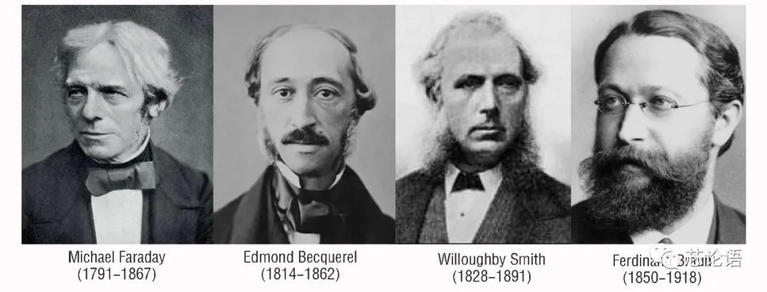
Figure 1. The four scientists who discovered semiconductor characteristics
(Faraday, Becquerel, Smith, Braun)
Although these four effects of semiconductors were discovered by scientists before 1880, the term semiconductor was not used until around 1911, when it was first introduced by J. Konigsberger and I. Weiss. Later, theories regarding semiconductor rectification, energy bands, and potential barriers were gradually completed through the efforts of many scientists.
In the following twenty years, several applications of semiconductors appeared worldwide. For example, from 1907 to 1927, American physicists successfully developed crystal rectifiers, selenium rectifiers, and copper(I) oxide (Cu2O) rectifiers. In 1931, selenium photovoltaic cells were successfully developed. In 1932, Germany successively developed semiconductor infrared detectors such as lead sulfide (PbS), lead selenide (PbSe), and lead telluride (PbTe).
In 1947, Bell Labs in the United States comprehensively summarized the aforementioned four characteristics of semiconductor materials. From 1880 to 1947, a span of 67 years, the research and application of semiconductor materials progressed very slowly due to the difficulty in purifying semiconductor materials to an ideal level. Subsequently, tetravalent elements such as germanium (Ge) and silicon (Si) became the focus of scientists’ attention and research. A few years after W. Shockley invented the germanium transistor, it was found that silicon was more suitable for producing transistors. Since then, silicon has become the most widely used semiconductor material, a trend that continues to this day. This is also why Northern California became known as “Silicon Valley” after becoming the center of the silicon industry.
Semiconductor materials have electrical conductivity between that of conductors and insulators; their resistance is much greater than that of conductors but much less than that of insulators. Their electrical properties can be artificially altered. Common semiconductor materials include silicon (Si), germanium (Ge), gallium arsenide (GaAs), silicon carbide (SiC), and gallium nitride (GaN).
2.The Invention of Vacuum Tubes (1906, 115 years ago)
In 1904, British physicist John Ambrose Fleming invented the world’s first vacuum tube, a vacuum diode, for which he obtained a patent.
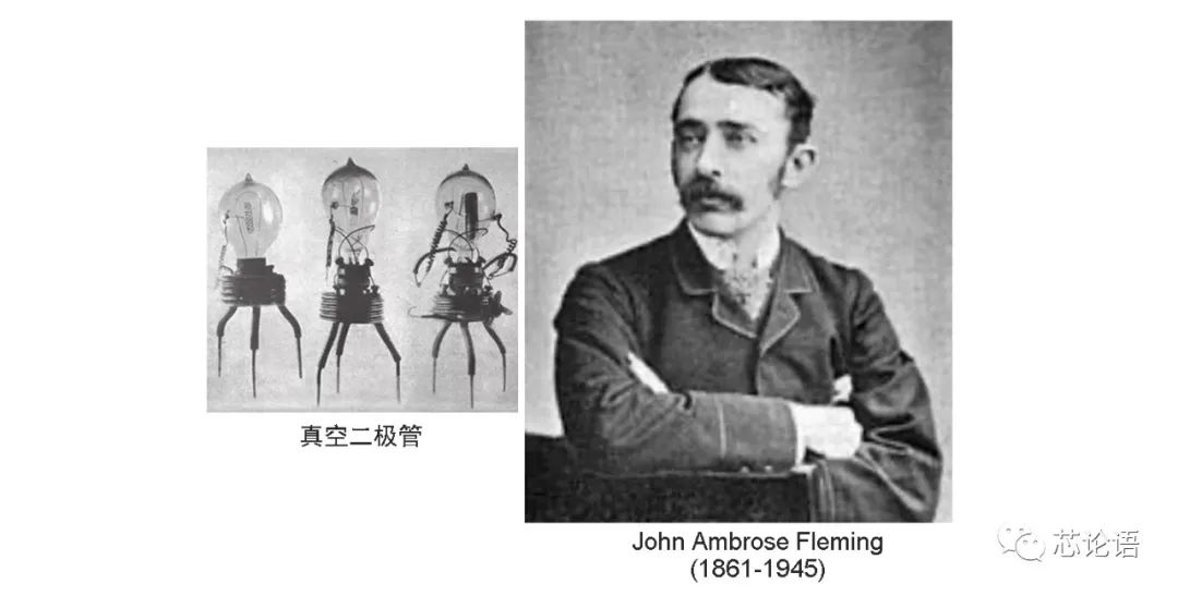
Figure 2. The vacuum diode invented by Fleming
In 1906, American engineer Lee de Forest built upon Fleming’s vacuum diode by adding a grid, inventing another type of vacuum tube, a vacuum triode, which allowed the vacuum tube to not only perform detection and rectification functions but also amplification and oscillation functions. De Forest obtained a patent for this invention on February 18, 1908.
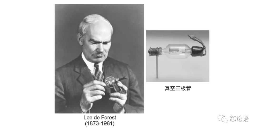
Figure 3. The vacuum triode invented by De Forest
The vacuum triode is considered the starting point of the electronics industry. Its application lasted for over 40 years. Due to the disadvantages of vacuum tubes, such as large size, high power consumption, and poor reliability, they were ultimately replaced by transistors.
3.The Invention of Transistors (1947, 74 years ago)
In 1947, John Bardeen, Walter Brattain, and William Shockley from Bell Labs in the United States invented the point-contact transistor, an NPN germanium (Ge) transistor, for which they won the Nobel Prize in Physics in 1956.
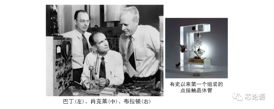
Figure 4. The trio who invented the transistor
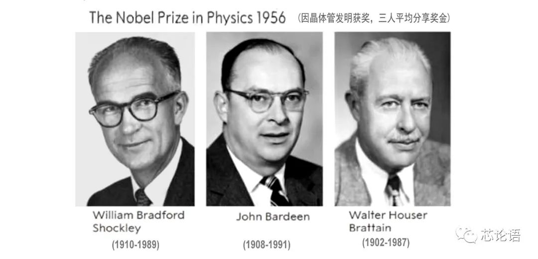
Figure 5. The trio who won the Nobel Prize in Physics in 1956
In 1950, after G.K. Teal and J.B. Little successfully researched the technology for growing large single-crystal germanium, W. Shockley created the first bipolar junction transistor—PN junction transistor in April 1950. This type of transistor is much more widely used than the point-contact transistor. Most transistors today are still of this PN junction type. The PN junction refers to the junction of a P-type semiconductor and an N-type semiconductor, where the P-type semiconductor has many holes and the N-type semiconductor has many electrons.
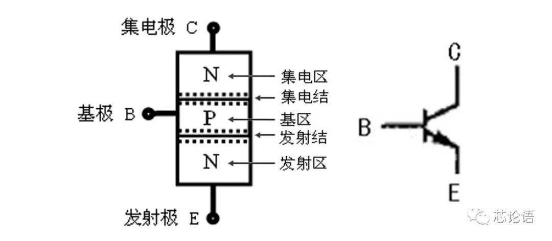
Figure 6. Schematic diagram of the PN junction transistor structure (left) and transistor symbol (right)
In 1952, the practical Junction Field-Effect Transistor (JFET) was manufactured. JFET is a type of transistor that controls current using an electric field effect. By 1960, someone proposed improving the performance of bipolar transistors with silicon dioxide, leading to the birth of the Metal-Oxide-Semiconductor (MOS) field-effect transistor. M. Atalla is also considered one of the inventors of the MOS field-effect transistor (MOSFET).
MOSFET announced its dominance in electronic technology and supported the cornerstone of today’s information society—the development of large-scale integrated circuits. In fact, field-effect transistors (FET) were invented by Julius Lilienfeld in 1925 and German physicist Oskar Heil in 1934, but practical transistor devices had not been manufactured until much later.
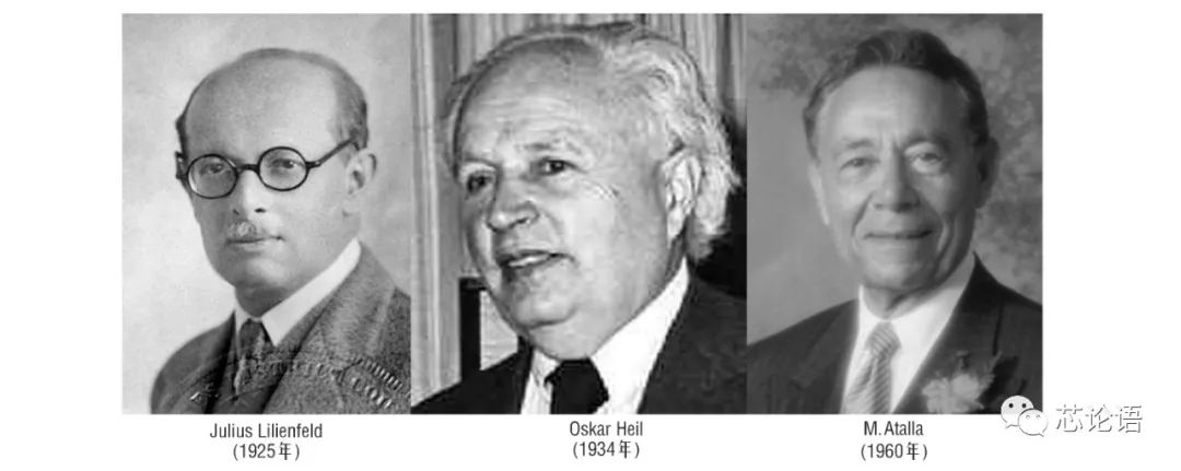
Figure 7. Contributors to the invention of MOSFET and the year of invention
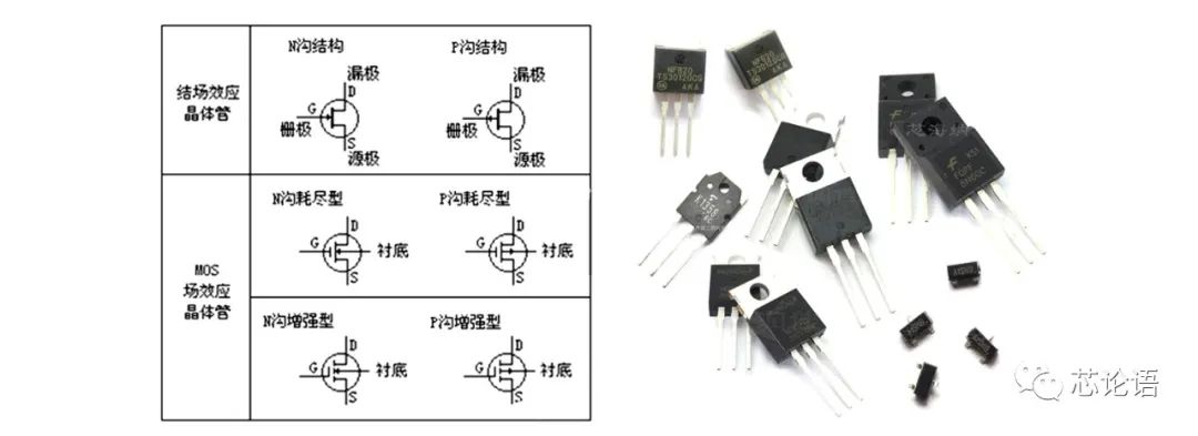
Figure 8. Classification and physical images of field-effect transistors (FET)
Transistors have evolved from bipolar to MOS types, from discrete devices to integration on chips, coupled with the use of different semiconductor materials, resulting in a wide variety of transistor types and categories. Transistors mainly serve the functions of small signal amplification, power amplification, and current switching, making them the most basic circuit components integrated in chips.
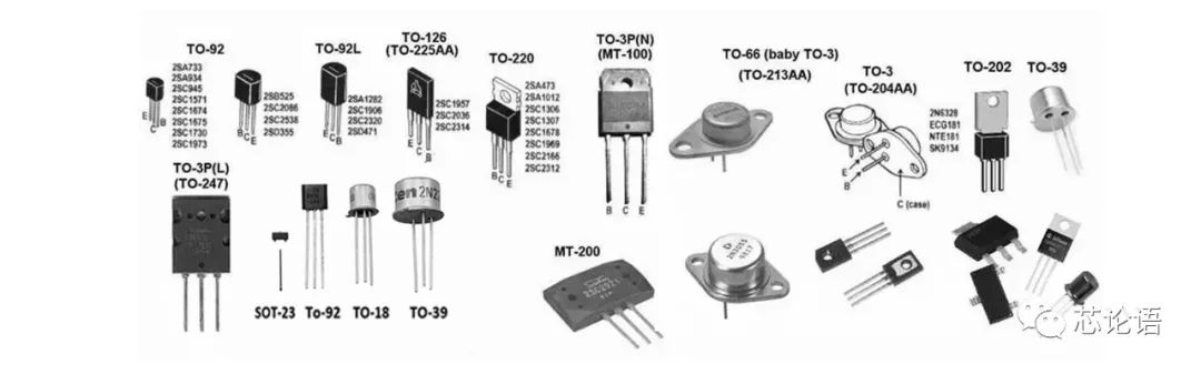
Figure 9. Classification of various transistors
The invention of the transistor marks the first milestone in the development of microelectronics technology. The invention of the transistor has ushered humanity into a rapidly developing electronic information age. To date, its application has lasted for 74 years.

Figure 10. Various packaging forms of discrete transistors
4.The Invention of Integrated Circuits (Chips) (1958, 63 years ago)
In 1950, Americans Russell Ohl and William Shockley invented the ion implantation process. In 1954, Shockley applied for a patent for this invention. Ion implantation is the process of ionizing impurities into ions and focusing them into an ion beam, which is accelerated in an electric field and injected into silicon materials to achieve doping of silicon materials, aimed at altering the electrical conductivity of silicon materials. Ion implantation is one of the earliest methods of semiconductor doping and is a fundamental process in chip manufacturing.
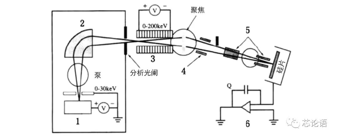
Figure 11. A brief schematic diagram of the principle of ion implantation
In 1956, American C.S. Fuller invented the diffusion process; diffusion is another method of doping, and it is also one of the fundamental processes in chip manufacturing.

Figure 12. A schematic diagram of a thermal diffusion device
Ion implantation and diffusion are two doping methods. Ion implantation is used to form shallow semiconductor junctions, while diffusion is used to form deeper semiconductor junctions. Doping is like adding seasoning to a dish; it is the process of “adding oil and vinegar” to semiconductor materials. A small amount of other substances is added to very pure semiconductor materials to make them impure; for semiconductor materials, the other substances are impurities, and the process of adding them is called doping. Doping is the process of adding a certain amount of other substances to semiconductor materials to artificially change the electrical properties of the semiconductor materials.
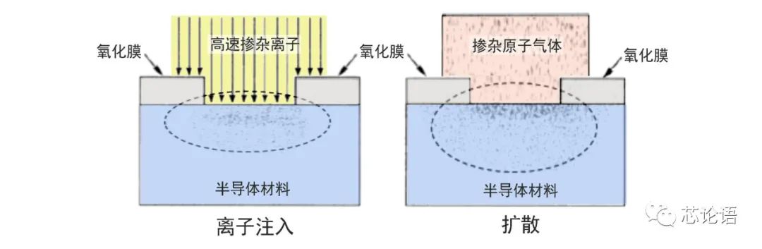
Figure 13. Schematic diagrams of two semiconductor doping methods
In 1958, Robert Noyce of Fairchild Semiconductor and Jack Kilby of Texas Instruments invented the integrated circuit within months of each other, marking the beginning of the history of microelectronics. Noyce invented a commercially producible integrated circuit based on Kilby’s invention, transitioning the semiconductor industry from the “invention era” to the “commercial era.”
Kilby received the Nobel Prize in Physics in 2000 for his invention of the integrated circuit. Noyce was one of the founders of Fairchild Semiconductor (established in 1957) and Intel Corporation (established in 1968). He was a great scientist and an important figure in the history of integrated circuits. Unfortunately, he did not receive support from his boss for his invention of the “negative resistance diode” while working at Shockley Labs, which was later awarded the Nobel Prize to Japanese scientist Leo Esaki; he passed away in 1990 without sharing the Nobel Prize in Physics with Kilby in 2000, missing out on the highest honor in technology twice. However, both are hailed as the fathers of integrated circuits.
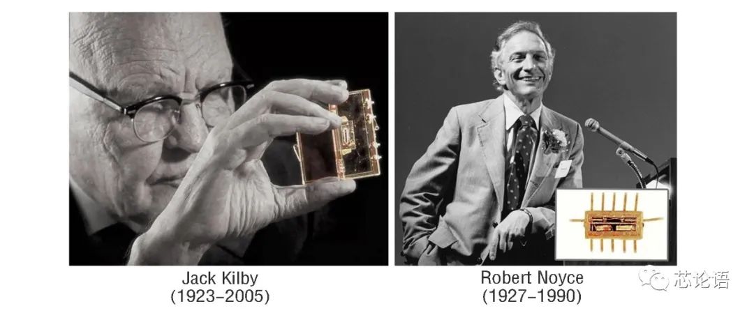
Figure 14. Kilby and Noyce with their invented chips
In 1959, Korean scientist Dawon Kahng and Dr. Simon Sze at Bell Labs invented the metal-oxide-semiconductor field-effect transistor (MOSFET), the first truly compact MOSFET and the first transistor that could be miniaturized and mass-produced, largely replacing JFET. MOSFET has had a profound impact on the development of the electronics industry.
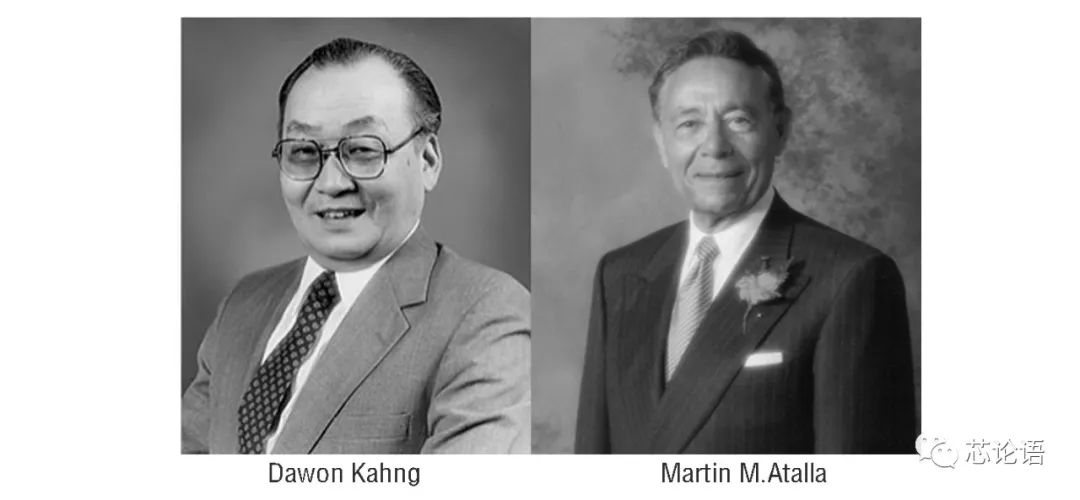
Figure 15. Dawon Kahng and Atalla invented MOSFET
5.Photolithography is the Soul of Chip Manufacturing (Invented 61 years ago)
In 1960, H.H. Loor and Christenson invented the epitaxy process. Epitaxy refers to growing a layer of single crystal material on single crystal semiconductor material with specific requirements, extending the original crystal.
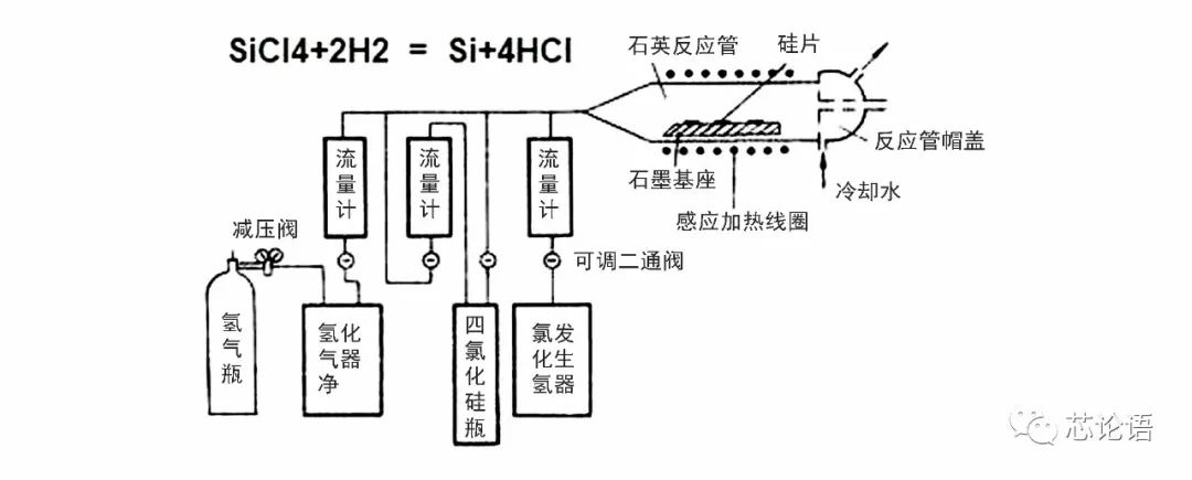
Figure 16. Schematic diagram of the principle of silicon vapor phase epitaxy growth
Was photolithography first applied in chip manufacturing in 1960? This is an important question that needs to be discussed in detail in this article. Photolithography is the soul technology of chip manufacturing. It is the advent of photolithography that has allowed silicon device manufacturing to enter the era of planar processing technology, leading to the rapid development of large-scale integrated circuits and microelectronics today.
In a general sense, the invention of photolithography technology should be traced back to the experiments with photosensitive materials and etching conducted by French scientist Joseph Nicephore Niepce in 1822, as well as the reproduction of the d’Amboise bishop sculpture he made in 1827. The photolithography referred to in this article specifically pertains to the photolithography technology used in the chip manufacturing process.
When was the photolithography process for chip manufacturing actually invented? The author finds that there are very few articles on this topic online, and even if there are articles, they are often brief. There are mainly two claims online: the first claim is that in 1960, H.H. Loor and E. Castellani invented the photolithography process. The second claim is that in 1970, E. Spiller and E. Castellani invented the photolithography process. The two claims differ by a decade. It is also difficult to find information online about how Loor, Castellani, and Spiller invented the photolithography process, and even their biographies are hard to find.
The author is more inclined to believe that 1960 should be the year of invention of photolithography. Because if photolithography was invented in 1970, then it would have been very difficult to manufacture semiconductor products (bipolar, FET, MOSFET transistors) and chips from pioneering companies such as Bell Labs, Fairchild, TI, RCA, and Intel during the decade from 1958 to 1970.
The author also believes that Fairchild Semiconductor should be the birthplace of photolithography technology. In 1958, several founders of Fairchild Semiconductor purchased three 16mm lenses from a camera store to create a stepping and repeating photographic device to make masks, improving the mask and photoresist. In June 1959, Robert Noyce proposed a technical idea in his diary, “Since we can use photolithography to manufacture single transistors, why can’t we use photolithography to mass-produce transistors?” “Putting multiple components on a single silicon wafer will enable internal connections of components in the process flow, thus reducing volume and weight, and lowering costs.” Therefore, Fairchild began to attempt to apply photolithography technology to the mass production of transistors. Noyce proposed the concept of “planar technology,” and Jean Hoerni was the one who turned this idea into a feasible “planar processing” technology.
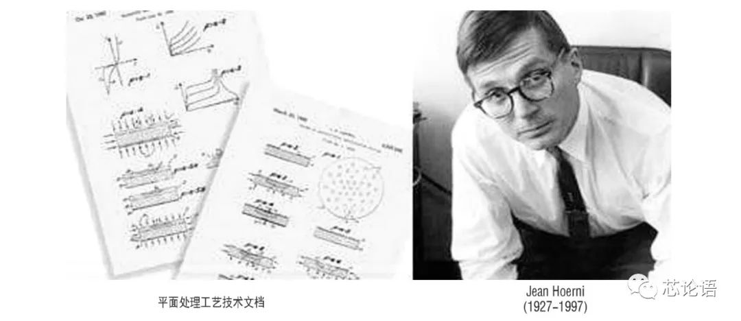
Figure 17. Hoerni and the technical documentation he wrote for planar processing technology
From the development timeline of photolithography machines, the 1960s saw contact photolithography and proximity photolithography; the 1970s saw projection photolithography; the 1980s saw step-and-repeat photolithography; and subsequently, step-and-scan photolithography, immersion photolithography, and today’s EUV photolithography. It is evident that the photolithography process for chip manufacturing could not have been invented in 1970.
Ion implantation, diffusion, epitaxy, photolithography, and other process technologies, along with vacuum coating technology, oxidation technology, and testing and packaging technology, form the main body of silicon planar processing technology, which can be simply described as the foundation of chip manufacturing. Without photolithography technology, there would be no today’s chip technology and industry, nor would there be our current information and intelligent society.
6.Chip Technology Continues to Mature and Rapidly Develops Along Moore’s Law
In 1962, Steven Hofstein and Frederic Heiman of RCA developed the first mass-producible Metal-Oxide-Semiconductor Field-Effect Transistor (MOSFET) and integrated 16 experimental MOS transistors onto a single chip, which is the first true MOS integrated circuit in the world.
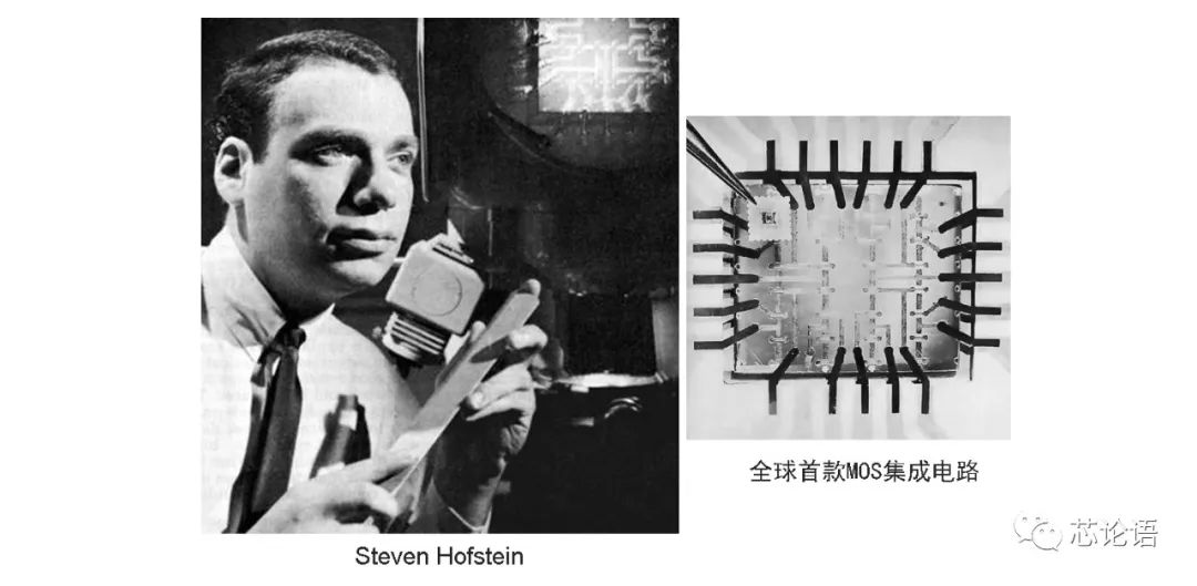
Figure 18. Hofstein and the world’s first MOS integrated circuit
In 1963, Frank M. Wanlass of Fairchild Semiconductor and Chinese-American C.T. Sah first proposed CMOS circuit technology. They connected N-MOS and P-MOS into a complementary structure, where the two polarities of MOSFETs operate alternately with almost no static current, making it suitable for logic circuits. In June 1963, Wanlass applied for a patent for CMOS, but shortly thereafter, he left Fairchild. The first CMOS circuit chip was developed by RCA. CMOS circuit technology laid a solid foundation for the development of large-scale integrated circuits. Today, over 95% of integrated circuit chips are manufactured based on CMOS technology.
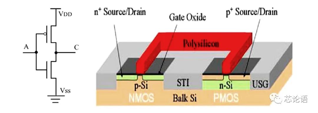
Figure 19. CMOS inverter circuit symbol and device model
In the same year, the circuit design genius Robert Widlar, aged 26 at Fairchild, designed the first integrated operational amplifier circuit μA702.
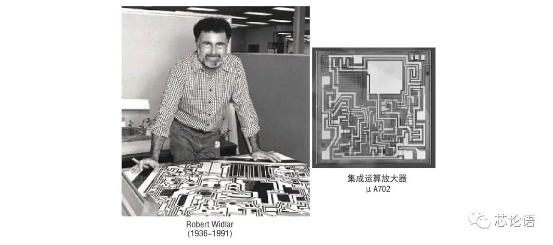
Figure 20. Fairchild Semiconductor μA702 operational amplifier chip
In 1964, one of the founders of Intel, Gordon Moore, proposed the famous Moore’s Law, predicting that the future development trend of chip technology is that the number of components that can be accommodated on a chip will double approximately every 18-24 months without changing the price, and performance will also double. The development of chip technology over the past 50 years has proven that Moore’s Law is basically accurate.
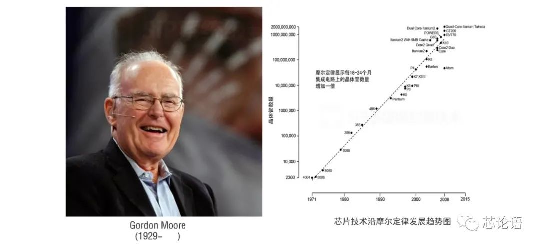
Figure 21. Moore, the trend chart of chip technology development along Moore’s Law
In 1966, RCA developed CMOS integrated circuits and the first 50-gate gate array chip.
In 1967, Applied Materials was established in the United States, which has now become the world’s largest semiconductor equipment manufacturer. In the fiscal year 2020, it achieved a revenue of 17.2 billion USD, with R&D investment reaching 2.2 billion USD, employing 24,000 people globally and holding 14,300 patents. Its business covers semiconductors, displays, solar energy, flexible coatings, automation software, etc. The following image summarizes the semiconductor business of Applied Materials.
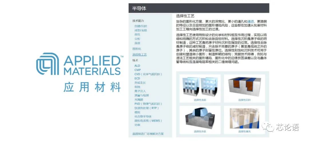
Figure 22. The semiconductor business of Applied Materials (Source: Applied Materials official website)
In 1967, Korean scientist Dawon Kahng and Dr. Simon Sze at Bell Labs jointly invented non-volatile memory. This is a floating-gate MOSFET, which is the basis for erasable programmable read-only memory (EPROM), electrically erasable programmable read-only memory (EEPROM), and flash memory.
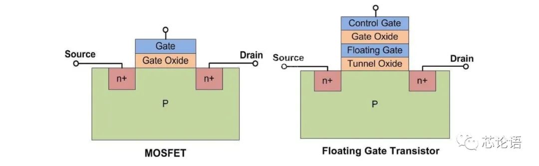
Figure 23. Comparison of ordinary MOSFET and floating-gate MOSFET
In 1968, Robert H. Dennard of IBM invented the single-transistor dynamic random-access memory (DRAM). The invention was titled “An Invention of a Transistor Dynamic RAM Cell.” The single-transistor DRAM was a groundbreaking invention that later became the standard for computer memory. Dennard was inducted into the National Inventors Hall of Fame in 1997 and received the IEEE Medal of Honor in 2009, the highest honor in the field of electrical and electronic engineering.
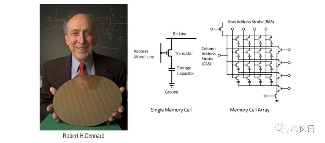
Figure 24. Dennard and the schematic diagram of single-transistor DRAM
The story continues.
Please look forward to Science Popularization: The Development History of Chip Technology Over 60 Years (Part 2).
Postscript: The 20-plus years from 1947 to 1968 marked the beginning of global chip technology and the electronics industry, during which innovative talents emerged, and impactful inventions were numerous. Inventions such as transistors, integrated circuits, silicon planar processing technology centered around photolithography, CMOS circuits, non-volatile memory, and single-transistor DRAM circuits laid the foundation for the rapid development of chip technology, paving the way for chip technology to advance along Moore’s Law. However, before humanity embarked on this broad road, it had already explored a rugged path for 114 years, from the understanding and discovery of semiconductors to the invention of transistors, including over 40 years of obsession with vacuum tubes. Technological progress cannot be achieved overnight; it is a gradual process of understanding, discovery, and maturation.
References:
1. The Story Behind the Invention of Field Effect Transistors, website www.circuitstoday.com: http://www.circuitstoday.com/the-story-behind-the-invention-of-field-effect-transistors
2. Heartfelt, The Inventor of MOSFET—Dr. Martin M.