The diameter of human hair is 70,000 nanometers, and the circumference is 220,000 nanometers. Manufacturing chips using a 5-nanometer process is akin to building 44,000 roads along a single strand of hair.
 Author: Liu Zhirong Source: Toutiao @铁塔-刘植荣
On May 15, 2020, the United States issued a chip ban against Huawei, which sparked widespread attention to chips among the Chinese populace. The ban took effect on September 15, preventing renowned chip manufacturers like TSMC, MediaTek, Qualcomm, Sony, Samsung, SK Hynix, and Micron from supplying chips to Huawei. On September 16, the Central Commission for Discipline Inspection of China stated on its official website that “the cutoff of Huawei’s chip supply might mark the beginning of a rebirth for China’s chip industry.”
We talk about chips every day, but do you really know what chips are?
1. The Invention of Chips Changed Human Lifestyles
On December 23, 1947, three scientists from Bell Labs in the United States, John Bardeen, William Shockley, and Walter Brattain, invented the germanium transistor, marking the entry of the electronic world into the semiconductor era. The three inventors of the transistor were awarded the Nobel Prize in Physics in 1956.
The 1950s were the golden age of semiconductors, during which almost all semiconductor materials and fundamental processes were developed.
On October 18, 1954, Texas Instruments invented the transistor radio, a radio with four transistors that was small enough to fit in a pocket.
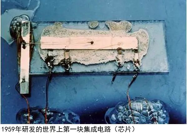
On September 12, 1958, Texas Instruments engineer Jack Kilby (1923-2005) invented the integrated circuit and successfully manufactured the world’s first integrated circuit, or chip, in 1959. This integrated circuit was etched with PNP transistors (triodes), resistors, and capacitors on a germanium wafer, connecting them into a circuit with external wires. This rudimentary integrated circuit opened the curtain on the chip industry and pushed human technological levels to new heights, fundamentally changing human lifestyles.
The continuous advancement of chip manufacturing technology has greatly reduced the cost of individual transistors. In 1959, a chip contained six transistors, costing about $10 each; in 1971, a chip had 2,000 transistors, costing about $0.30 each; by 2004, a chip could contain over 10 billion transistors, with the price of a single transistor dropping to one billionth of a dollar. The improvement in cost-effectiveness allowed chips to enter the homes of ordinary people.
Chips can be considered the greatest invention of the 20th century, with many other inventions built upon the foundation of chips. Today, we live in a world surrounded by chips, and without them, we cannot move forward.
Everyday life is inseparable from chips; smartphones, computers, smartwatches, and other smart devices contain chips. Network devices and computer peripherals like optical modems, routers, USB drives, storage cards, and external hard drives have chips. Personal identification documents like ID cards, passports, bank cards, shopping cards, and consumer cards contain chips. Household appliances such as televisions, sound systems, projectors, chargers, LED lights, electronic scales, air conditioners, refrigerators, microwave ovens, induction cookers, and water heaters also contain chips, as do access control systems, surveillance cameras, and solar batteries. If someone invented a code that disabled all chips in the world, human life would come to a standstill.
Jack Kilby won the Nobel Prize in Physics in 2000 for his invention of the chip. He was also the inventor of the handheld calculator and thermal printer. When referred to as a scientist, Kilby humbly stated, “Scientists are those who explain things and have great ideas; I am a problem solver, just an engineer, whose job is to invent new processes, create new products, and profit from those inventions.”
2. To Understand Chips, One Must First Know About the ‘PN Junction’
As mentioned above, creating diodes, transistors, resistors, capacitors, and other electronic components on semiconductor materials and connecting them with wires constitutes an integrated circuit, also known as a chip. To understand chips, one must first understand the ‘PN junction,’ which is the core of semiconductor technology.
When semiconductor materials are doped with pentavalent elements, the electron concentration increases, forming an N-type semiconductor; when doped with trivalent elements, the hole concentration increases, forming a P-type semiconductor. A ‘hole’ refers to an empty space left behind when a covalent bond’s electron gains energy and escapes its confinement.
When P-type and N-type semiconductors come into close contact, negatively charged electrons and positively charged holes diffuse toward each other; this diffusion creates an internal electric field at the junction, which inhibits further diffusion and causes electrons and holes to drift back. When the diffusion speed of electrons and holes matches their drift speed, a dynamic equilibrium is reached, forming the ‘PN junction’ at the contact surface of the P-type and N-type semiconductors.
The main characteristic of the ‘PN junction’ is its ‘unidirectional conductivity.’ If the P-type semiconductor is connected to the positive terminal and the N-type to the negative terminal, current can pass through the PN junction; if the N-type is positive and the P-type is negative, current cannot flow through the PN junction. The binary system used in computers is determined by the properties of the ‘PN junction,’ where current passing through the junction represents ‘1’ and current not passing through represents ‘0.’
The ‘PN junction’ is essentially a diode. If a P-type semiconductor is sandwiched between two N-type semiconductors, it forms a transistor, which is the aforementioned PNP transistor. Conversely, if an N-type semiconductor is sandwiched between two P-type semiconductors, it forms an NPN transistor.
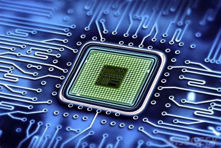
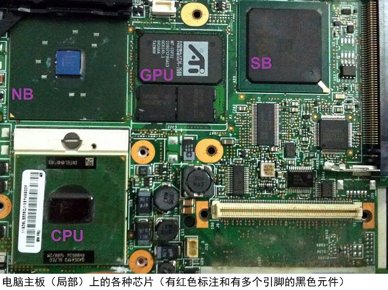
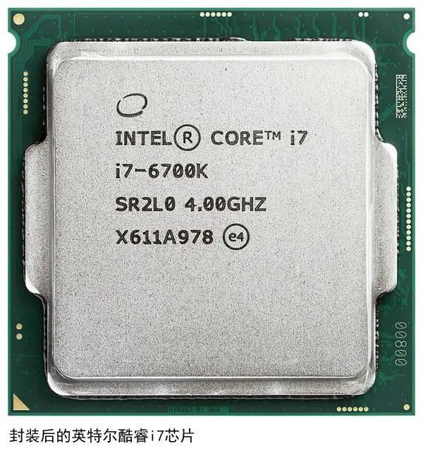
Ordinary people cannot see the ‘true form’ of a chip; chips are as small as human dandruff, and the largest are only about the size of a fingernail. They are so thin that they must be encapsulated in a sealed shell to connect to external circuits. Opening a computer, television, or other electrical appliance reveals a large circuit board with many electronic components; those components with multiple pins are chips, and these pins connect to the chip’s input and output terminals, some located on the sides of the chip package, some on the four sides, and others arranged in dense matrices on the bottom, with over 1,000 pins.
3. Making Chips is Like Carving the Earth and All Its Roads and Buildings on a Grain of Rice
Here, we need to mention a concept known as ‘Moore’s Law.’ In 1965, Gordon Moore, one of the founders of the world-renowned chip manufacturer Intel, proposed that the number of transistors on a single chip would double every year. He later corrected this to every two years. This prediction has been largely validated by practice. In 2011, Intel’s Core i7 chip contained 2.27 billion transistors. Currently, some high-end chips have transistor counts exceeding hundreds of billions. A few years ago, the semiconductor company Cerebras Systems produced an AI chip, the WSE, using TSMC’s 16-nanometer process, which integrated 1.2 trillion transistors!
‘Process’ refers to the width of the transistor gate on the chip, which can be understood as the size of the transistor. The smaller the process, the more transistors can be made on a chip, leading to a larger scale of integrated circuits.
The continuous improvement in chip processing speed is due to the increasing integration of chips. The higher the integration, the smaller the electronic components, and the shorter the wires between components, reducing the time it takes for current to flow and thus decreasing energy consumption and increasing processing speed.
There are three ways to increase the number of transistors on a chip: one is to increase the chip area, the second is to reduce the size of the transistors, and the third is to make the integrated circuits three-dimensional. Increasing the chip area is generally not considered, as it would increase energy consumption and reduce efficiency. Currently, the latter two methods are primarily used to increase the number of transistors on chips.
Chip manufacturing belongs to the microscopic world, where electronic components are as small as a few atoms or molecules and are measured in smaller units like nanometers and angstroms. The smallest scale on a ruler is a millimeter, where 1 millimeter equals 1,000 micrometers, 1 micrometer equals 1,000 nanometers, and 1 nanometer equals 10 angstroms. The diameter of human hair is 70,000 nanometers, and the circumference is 220,000 nanometers. Using a 5-nanometer process to manufacture chips is like building 44,000 roads along a single strand of hair.
Reducing the size of electronic components has its limits, prompting the idea of building multi-layer integrated circuits on a single chip to increase the number of transistors. This is akin to residential buildings; single-story houses accommodate fewer residents, while multi-story buildings can house many more. However, stacking integrated circuits is much more complex than constructing buildings. The layouts of different floors in buildings are the same, while the circuits on different layers of a chip are different, and the connections between layers are exceptionally intricate.
To further illustrate, manufacturing chips is like carving a complete Earth on a grain of rice, including all the roads and buildings on Earth. The roads represent the wires on the chip, and the buildings represent the electronic components on the chip. Through this analogy, readers can imagine how complex and challenging chip manufacturing is.
4. Purification of Silicon is the Foundation of the Chip Industry
There are many semiconductor materials, but in practice, over 90% of them use silicon due to its melting point of 1,415 degrees Celsius, which allows for high-temperature processes in chip fabrication.
Silicon is derived from sand, but to turn sand into silicon suitable for chip manufacturing, extremely high purity is required. We refer to gold with a purity of 99.99% as pure gold (four nines), but the purity of silicon for chip manufacturing must reach at least eleven nines, meaning that there can be no more than one impurity atom in every billion silicon atoms. This level of purity was achieved by Bell Labs in the United States in 1955. Currently, a chip contains trillions of electronic components, requiring even higher purity, at least thirteen nines. This is the foundation of chip manufacturing; without mastering silicon purification technology, it is impossible to produce chips!
Readers may wonder why silicon for chip manufacturing requires such high purity. The electronic components on chips are extremely small, and if a chip made with a 5-nanometer process contains even a 1-nanometer impurity, the entire chip will be rendered useless. To illustrate, if a road is 40 meters wide and there is a 1-meter wide boulder in the middle, cars can avoid it without causing traffic congestion. However, if a road is only 5 meters wide, a 1-meter boulder in the middle will block the road completely.
Therefore, chip manufacturing requires not only high purity silicon but also a dust-free environment at every stage of the manufacturing process, with cleanliness levels 100,000 times that of a hospital operating room, and much of the process is conducted in a vacuum. For this reason, chip manufacturing plants did not need to stop operations during the COVID-19 pandemic, as workers were fully protected from head to toe, and some protective suits even had their own breathing systems to prevent contaminants from the human body from affecting the chips.
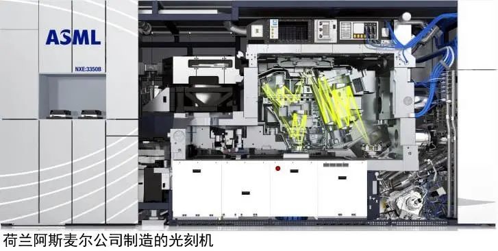
5. Photolithography Machines are Essentially Integrated Circuit Projectors
The term “photolithography machine” is inaccurately translated and can be misleading, as many people mistakenly believe that photolithography machines “engrave” integrated circuits onto the surface of silicon wafers through physical contact, like a computer engraving text. In reality, chips are not “engraved” but “projected”. Therefore, calling photolithography machines “integrated circuit projectors” is more accurate.
When the wafers used to manufacture chips enter the photolithography process, the photolithography machine projects the integrated circuit design onto the surface of the photoresist on the wafer through a mask. After exposure, the photoresist is etched using chemical solutions, and then washed, resulting in the formation of the integrated circuit pattern. The photolithography process is analogous to developing a photograph, where light passes through a negative to sensitize the photographic paper, which is then developed and fixed in chemical solutions.
A single chip undergoes dozens or even hundreds of photolithography steps, and several weeks of additional processes are required before it can enter the packaging stage.
Chip manufacturing technology is advancing rapidly, but most core technologies in chip manufacturing originated from Bell Labs, whose contributions to the information technology revolution will be remembered in history.
7. Can Chips Be Manufactured Just with Photolithography Machines?
Many readers are interested in photolithography machines, believing that having a photolithography machine is sufficient to produce chips. However, this is not the case; although photolithography machines play a crucial role in chip manufacturing, they are merely one step in the more than 1,000 processes involved in chip production. Without mastering other processes, it is impossible to produce chips even with a photolithography machine.
In 1961, the American company GCA produced the world’s first photolithography machine. Currently, there are seven companies in four countries that can manufacture photolithography machines: ASML from the Netherlands, Intel, Ultra Technology Semiconductor, and Rudolph from the United States, Nikon and Canon from Japan, and Süss MicroTec from Germany.
As mentioned earlier, the foundation of the chip industry is materials, specifically the purification of silicon; without mastering silicon purification technology, it is impossible to produce silicon of chip-grade purity, making chip production unfeasible.
Moreover, with trillions of electronic components on a chip, such a vast circuit cannot be drawn by hand; electronic design automation (EDA) software must be used. EDA is a comprehensive application of multiple natural sciences, monopolized by three companies: Cadence, Synopsys, and Mentor Graphics in the United States.
EDA plays a decisive role in chip manufacturing, as the functionality and integration of chips depend entirely on the design capabilities of EDA. Having high-purity silicon and a photolithography machine is insufficient; without EDA or the ability to use EDA, it is still impossible to produce chips.