In modern ARM CPU architecture, pipeline technology is one of the key means to enhance processor performance. It divides the instruction execution process into multiple stages, allowing multiple instructions to be in different execution stages at the same time, thus achieving parallel processing of instructions and greatly improving the CPU’s execution efficiency. However, in actual operation, ARM CPU pipelines also face some performance bottlenecks that affect their full performance.
- 1.1.
- 1.2.
-
ARM CPU Pipeline Working Principle
1.1 Pipeline Introduction
The ARM CPU pipeline typically consists of multiple stages, here we introduce a simple five-stage pipeline. It consists of the following five steps:1. Instruction Fetch (IF);2. Instruction Decode (ID);3. Execute (EXE);4. Memory Access (MEM);5. Write-Back (WB).
| Instruction | Clock Cycle | |||||||
| 1 | 2 | 3 | 4 | 5 | 6 | 7 | 8 | 9 |
| X | IF | ID | EXE | MEM | WB | |||
| X+1 | IF | ID | EXE | MEM | WB | WB | ||
| X+2 | IF | ID | EXE | MEM | WB | |||
| X+3 | IF | ID | EXE | MEM | WB | |||
| X+4 | IF | ID | EXE | MEM | WB |
Diagram of the five-stage pipeline
1) Instruction Fetch Stage
In this stage, the CPU reads instructions from memory. Based on the memory address pointed to by the program counter (PC), the corresponding instruction is loaded from memory into the Instruction Cache. If the instruction cache hit occurs, the fetch speed will be very fast; if not, it needs to read the instruction from main memory, which will introduce significant delay. The instruction fetch stage is the starting point of the pipeline, and its efficiency directly affects the execution of subsequent stages.
2) Decode Stage
After the instruction fetch is complete, the instruction enters the decode stage. In this stage, the CPU parses the instruction, identifying the opcode, operands, and addressing mode, etc. The decoder determines the specific operation of the instruction and the resources needed based on this information, preparing for the subsequent execution stage. The accuracy and speed of decoding are crucial for the smooth operation of the entire pipeline.
3) Execute Stage
The execute stage is where the instruction actually performs operations. Based on the operation information parsed in the decode stage, the CPU’s arithmetic logic unit (ALU) executes the corresponding arithmetic, logical operations, or data transfer operations. For example, for an addition instruction, the ALU performs addition on two operands; for a data transfer instruction, it transfers data from one register to another or to a memory location.
4) Memory Access Stage
If the instruction involves memory access (such as loading or storing data), the corresponding operation is completed in the memory access stage. For load instructions, the CPU reads data from memory; for store instructions, it writes data to memory. The performance of the memory access stage is influenced by the speed of memory access, and high memory latency can lead to pipeline stalls.
5) Write-Back Stage
After the execution and memory access operations are completed, the results are written back to the registers or memory. If the result needs to update a register, it will write the result into the corresponding register; if it involves memory operations, it will write the updated data back to memory. The write-back stage ensures that the results of instruction execution can be correctly saved, providing accurate data for subsequent instruction execution.Through pipeline technology, ideally, when one instruction completes the instruction fetch, the next instruction can enter the fetch stage, while the previous instruction sequentially enters the subsequent stages, achieving overlapping execution of multiple instructions and greatly improving CPU throughput.
1.2 Pipeline Optimization
To improve CPU pipeline efficiency, modern CPU designs adopt various advanced technologies, mainly including the following categories:
1) Superscalar and Multiple Issue Techniques
Superscalar technology allows the CPU to issue multiple instructions to different execution units simultaneously in each clock cycle, thereby increasing instruction-level parallelism (ILP). Multiple issue techniques further enhance parallel processing capabilities by increasing hardware resources (such as execution units and decoders).
| Instruction | Clock Cycle | |||||
| 1 | 2 | 3 | 4 | 5 | 6 | 7 |
| X | IF | ID | EXE | MEM | WB | |
| X+1 | IF | ID | EXE | MEM | WB | WB |
| X+2 | IF | ID | EXE | MEM | WB | |
| X+3 | IF | ID | EXE | MEM | WB | |
| X+4 | IF | ID | EXE | MEM | WB | |
| X+5 | IF | ID | EXE | MEM | WB |
Diagram of a simple dual-issue superscalar CPU pipeline
2) Out-of-Order Execution (OoOE)
Out-of-order execution allows independent instructions to be executed first by dynamically scheduling instructions, reducing stalls in the pipeline caused by data dependencies. Its key components include register renaming, instruction schedulers, and rollback mechanisms.For example:
- Load Instruction (LOAD): LOAD R1, 0(R2)
- This instruction may need to wait for memory access to complete, which usually incurs a delay.
- SUB R5, R6, R7
- MUL R8, R9, R10
- These two instructions do not depend on R1, so they can be executed before the LOAD instruction completes, thus reducing pipeline stalls.
- This instruction needs to wait for the LOAD instruction to complete and obtain the value of R1 before it can execute.
3) Branch Prediction and Speculative ExecutionBranch prediction reduces stalls in the pipeline caused by branch instructions by predicting the direction of branch instruction execution (jump or not jump). Modern CPUs use complex branch prediction algorithms (such as dynamic prediction, historical information prediction, etc.) to improve prediction accuracy.Speculative execution is an instruction execution strategy based on branch prediction results. The processor executes instructions ahead of time based on the predicted results of branch prediction; if the prediction is correct, the execution results are retained; if the prediction is wrong, these results are discarded, and the correct instructions are re-executed. The purpose of speculative execution is to further reduce stalls in the pipeline caused by branch instructions, thereby improving performance.For example:
if (a < b) fun1();else fun2();When it is unknown whether a < b is true or false, the CPU executes fun1() or fun2() based on the branch prediction results.
4) Instruction Prefetching and Cache Optimization
Instruction prefetching is a technique that predicts the instructions the CPU may need in the future and loads them into the instruction cache in advance. Its purpose is to reduce stalls in the pipeline caused by instruction cache misses, thereby improving instruction execution efficiency. Additionally, optimizing cache design (such as increasing cache size, improving cache coherence protocols) can significantly enhance pipeline efficiency.
1. Instruction Prefetching
The goal of instruction prefetching is to reduce the latency of instruction cache misses, ensuring that the processor can quickly obtain instructions when needed. Common instruction prefetching techniques include:(1) Next-line PrefetchingThe simplest prefetch strategy, based on the principle of spatial locality, assumes that the program will execute instructions sequentially. It will prefetch the next line of the cache where the current instruction is located.(2) Fetch-directed PrefetchingUtilizes branch predictors to recursively predict future control flows, thereby prefetching instruction blocks in advance. By introducing a Fetch Target Queue (FTQ), the prefetcher can obtain instructions from the L2 cache and temporarily store them in a fully associative buffer.(3) Prescient PrefetchUtilizes auxiliary threads or parallel resources to execute critical calculations and control transfers in advance, assisting the main thread. This method can effectively utilize the processor’s idle resources and improve prefetch efficiency.(4) Speculative ThreadingBy identifying critical execution information, it sends instruction prefetch requests in advance. It can traverse multiple instruction fetch discontinuities but is limited by single instruction granularity and has limited foresight capability.
2. Cache Optimization
The goal of cache optimization is to reduce cache miss rates and improve cache utilization. Common optimization techniques include:(1) Data PrefetchingBased on the program’s data access patterns, it loads data into the cache in advance. Common data prefetch strategies include:
- Stride-based and Stream Prefetching: Suitable for scenarios like array traversal.
- Address Correlation-based Prefetching: Predicts future data that may be accessed by analyzing the address patterns of data access.
- Execution-based Prefetching: Obtains critical data through auxiliary threads or by executing part of the code in advance.
(2) Cache Replacement AlgorithmsWhen the cache is full, it is necessary to decide which data should be replaced. Common algorithms include:
- Least Recently Used (LRU)
- First In First Out (FIFO)
- Random Replacement
(3) Multi-level Cache DesignModern processors typically use multi-level caches (L1, L2, L3, etc.), each with different capacities and speeds. Multi-level cache design can reduce access latency while effectively managing storage resources.(4) Cache CoherenceIn multiprocessor systems, it is necessary to ensure that the data in different processors’ caches remains consistent. Common solutions include cache coherence protocols (such as MESI protocol).
3. Applications of Instruction Prefetching and Cache Optimization
(1) Software LevelDevelopers can manually prompt the CPU to load data in advance by using explicit prefetch instructions (such as _mm_prefetch). For example, when processing arrays, they can prefetch the next batch of data in advance to reduce memory access latency.(2) Hardware LevelModern processors support hardware-level prefetching techniques, such as the prefetching function in the L1 instruction cache. Additionally, cache allocation techniques (CAT) allow system administrators to allocate specific cache areas for critical tasks, reducing interference from other tasks.
4. Challenges of Instruction Prefetching and Cache Optimization
- Prefetch Accuracy: If the prefetched data or instructions are not actually needed, it may waste resources and even pollute the cache.
- Prefetch Overhead: The prefetch operation itself consumes processor resources; if the overhead is too large, it may offset performance gains.
- Cache Coherence Issues: In multiprocessor systems, prefetched data needs to maintain consistency; otherwise, it may lead to program execution errors.
5) Register Renaming
The purpose of pipeline design is to allow each stage to process different instructions simultaneously, thereby improving overall processor performance. However, pipeline design also brings new problems, one of which is data hazards.Data hazard issues: In pipelines, a data hazard occurs when the data needed by an instruction is not yet ready, causing pipeline stalls. Common data hazards include:
- Read After Write (RAW): Also known as “true dependency,” it refers to a situation where one instruction needs to read the result of another instruction that has not yet completed writing.
- Write After Write (WAW): This occurs when one instruction needs to write to a register, but that register has not yet been completed by the previous instruction.
- Write After Read (WAR): This occurs when one instruction needs to write to a register, but that register has not yet been read by the previous instruction.
These conflicts can lead to pipeline stalls, reducing processor performance.Register renaming is a technique to solve WAW and WAR hazards. Its core idea is to allocate multiple physical register copies for each logical register and dynamically assign these copies through a renaming mechanism to avoid pipeline stalls caused by register conflicts.Specific process:
- Logical Registers and Physical Registers:
- Logical Register: The registers defined in the program, such as R1, R2, etc.
- Physical Register: The actual copies of registers owned by the processor, usually more than logical registers.
- When an instruction needs to write to a logical register, the processor allocates a new physical register and maps the logical register to this new physical register.
- For read operations, the processor looks up the physical register currently mapped to the logical register and reads data from it.
- When the instruction completes writing back, the processor updates the mapping relationship between the logical register and the physical register.
For example:Suppose there is a piece of code:
ADD R1, R2, R3 // R1 = R2 + R3SUB R4, R1, R5 // R4 = R1 - R5Without register renaming, the SUB instruction needs to wait for the ADD instruction to complete writing back R1, which causes pipeline stalls.With register renaming:
- When the ADD instruction starts executing, the processor allocates a new physical register P1 for R1.
- When the SUB instruction starts executing, the processor allocates another new physical register P2 for R1.
- When the ADD instruction completes writing back, the logical register R1 is mapped to the physical register P1.
- The SUB instruction can directly read the value of P1 without waiting for the ADD instruction to complete writing back.
Advantages of Register Renaming
- Eliminates WAW and WAR hazards: By allocating multiple physical copies for each register, it avoids pipeline stalls caused by register conflicts.
- Improves pipeline efficiency: Reduces stalls in the pipeline, improving overall processor performance.
- Supports out-of-order execution: Register renaming is the basis of out-of-order execution (OoOE), allowing the processor to dynamically adjust the execution order of instructions, further optimizing performance.
The implementation of register renaming usually relies on the following components:
- Rename Table: Used to record the mapping relationship between logical registers and physical registers.
- Free List: Used to manage available physical registers.
- Renaming Logic: During instruction decoding, it dynamically allocates physical registers based on the current mapping relationship and instruction requirements.
6) SIMD and Vectorization Optimization
SIMD (Single Instruction Multiple Data) technology allows the CPU to process multiple data simultaneously, suitable for computing tasks with high data parallelism. Through vectorization optimization, performance can be significantly improved.
7) Compiler Optimization
Modern compilers (such as GCC and Clang) reduce data dependencies and improve instruction-level parallelism through techniques like instruction reordering and loop unrolling.
With this foundational knowledge, let’s take a look at a practical CPU microarchitecture.
2. ARM CPU Microarchitecture Introduction
Here we introduce the CPU microarchitecture using the ARM Cortex-A77 microarchitecture as an example.
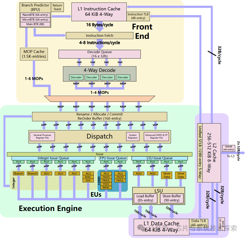 Diagram of ARM Cortex-A77 Core MicroarchitectureThe Cortex-A77 is the successor to the Cortex-A76. Similar to the A76, the A77 is also aimed at 7nm technology, but it aims to maximize the instructions per cycle (IPC) through a series of significant improvements while maintaining the same frequency range. Arm has achieved this goal by significantly enhancing instruction-level parallelism (ILP) and adopting a wider pipeline.
1) Pipeline
The Cortex-A77 is a complex 6-way superscalar out-of-order execution processor, with a backend supporting 10-way issue. Its pipeline has a total of 13 stages, with a minimum penalty of 10 cycles for branch prediction errors. The A77 is equipped with a 64 KiB Level 1 instruction cache (L1I) and a 64 KiB Level 1 data cache (L1D), as well as a configurable private Level 2 cache (L2) that supports 256 KiB (1 bank) or 512 KiB (2 banks).
2) Frontend
Each cycle, the A77 can fetch up to 32 bytes of instructions from the L1 instruction cache. The instruction fetch unit works in conjunction with the branch prediction unit to ensure that the instruction flow is continuously prepared for fetching. Additionally, the A77 is equipped with a return stack for storing return addresses of branch instructions and instruction set states (AArch32/R14 or AArch64/X30). When encountering return instructions (such as AArch64’s ret), the return stack pops the corresponding address.
3) Branch Prediction Unit
Maintaining a continuous supply of instruction flow is the task of the branch prediction unit (BPU). Similar to Enyo (A76), the A77’s branch prediction unit is decoupled from the instruction fetch unit, allowing it to run in parallel and predict branches in advance, thereby hiding the latency of branch prediction. Due to increased instruction fetch bandwidth, Arm has also doubled the instruction window size of the branch predictor to 64 bytes/cycle, enabling it to stay ahead of the instruction flow. The main branch target buffer (BTB) of the A77 has increased by 33% compared to the A76, reaching a depth of 8K entries. Arm states that this improvement directly enhances the performance of various real-world workloads. The BPU includes three stages to reduce latency, including a 64-entry micro BTB and a 64-entry nano BTB (the latter increased from 16 entries to 4 times its size).
4) L1 Instruction Cache
The L1 instruction cache of the A77 is fixed at 64 KiB, designed with a virtual index and physical tag (VIPT), but behaves like a physical index, physical tag (PIPT) 4-way set associative cache. L1I supports optional parity protection and employs a pseudo least recently used (pseudo-LRU) cache replacement policy. The read interface width between the instruction cache and the L2 cache is 256 bits, allowing for up to 16 bytes of data to be transferred from the shared L2 cache to the L1I cache each cycle.
5) Instruction Decoding
From the instruction fetch unit, up to 4 32-bit instructions can be sent to the decode queue (DQ) each cycle. This is twice that of the A76 and is the widest pipeline design by Arm at that time. For 16-bit Thumb instructions, up to 8 instructions can be decoded each cycle. The A77’s decoder is 6-way, capable of decoding up to 4 instructions into relatively complex macro operations (MOPs) each cycle. On average, the number of MOPs is about 6% more than the number of instructions. The entire decoding process is divided into two cycles: one for alignment and the other for decoding.
6) Backend
The backend of the A77 is responsible for executing out-of-order operations. Its design is mainly inherited from the Cortex-A76 but has been significantly expanded in width and depth.
7) Renaming and Allocation
From the frontend, up to 6 macro operations can be sent to the renaming unit each cycle. The A77 can simultaneously handle up to 160 instructions, which is 25% wider than all processors since its predecessor, the Cortex-A57. Arm has pointed out that a 10% increase in reorder buffer (ROB) capacity can yield a performance improvement of about 1-1.25%. Therefore, the 25% increase in A77 is expected to bring about a 2.5-3% performance improvement. Macro operations are broken down into micro-operations (µOPs) and scheduled for execution. The number of µOPs generated by MOPs has increased by about 20%. Subsequently, µOPs are sent to the instruction issue unit, which controls when to dispatch µOPs to the execution pipeline. µOPs are allocated to 8 independent issue queues (a total of 120 entries).
8) Execution Units
The backend issue width of the A77 is 12-way, which is a 50% increase over A76. This allows for up to 12 µOPs to be executed per cycle, with 10 µOPs entering the execution units and 2 µOPs entering the memory data pipeline. The execution units of the A77 are divided into three clusters: integer, advanced SIMD, and memory.Integer cluster: Contains 6 pipelines, which is an increase of 2 compared to A76. One improvement of the A77 is the unification of issue queues. Previously, each pipeline had its own issue queue, but in the A77, the integer cluster adopts a unified issue queue, improving efficiency. The A77 also adds a fourth general-purpose math ALU, supporting typical 1-cycle simple math operations and some 2-cycle complex operations. In total, there are 3 simple ALUs for arithmetic and logical data processing operations and a fourth port that supports complex arithmetic (such as MAC, DIV). The A77 also adds a second branch ALU, doubling branch throughput.Advanced SIMD/Floating Point Cluster: Contains 2 ASIMD/FP execution pipelines, the same as A76. The improvement lies in the unification of issue queues, similar to the integer cluster, the ASIMD cluster now also adopts a unified issue queue, improving efficiency. The ASIMD pipeline width of the A77 is 128 bits, supporting 2 double-precision operations, 4 single-precision operations, 8 half-precision operations, or 16 8-bit integer operations. These pipelines can also execute encryption instructions (additional authorization required). Compared to A76, the A77 adds a second AES unit to increase the throughput of encryption operations.
9) Memory Subsystem
The A77 includes two ports, each equipped with address generation units, supporting load and store operations. One significant improvement of the A77 is the way it handles storing data. Previously, the two memory data pipelines shared the issue ports of the integer ALU, but in the A77, the memory data pipelines now have independent dedicated ports, effectively doubling the load-store issue bandwidth.L1 data cache is fixed at 64 KiB, supporting optional ECC protection for every 32 bits. It is designed with a virtual index and physical tag, behaving like a physical index, physical tag 4-way set associative cache. L1D cache employs pseudo LRU replacement policy, with the fastest load-to-use latency of 4 cycles, having two read ports and one write port, supporting up to 2 16-byte loads or 1 32-byte store per cycle. The A77 supports up to 20 outstanding non-prefetch misses. The load buffer depth is 85 entries, and the store buffer depth is 90 entries. The A77 can handle up to 175 memory operations simultaneously, which is about 10% more than its instruction window.The L2 cache of the A77 can be configured to 128 KiB, 256 KiB, or 512 KiB (using two 256 KiB banks). It employs a dynamic bias replacement strategy and supports ECC protection for every 64 bits. The L2 cache strictly contains L1 data cache but does not include L1 instruction cache. The write interface width of the L2 cache is 256 bits, and the read interface width is also 256 bits. The fastest load-to-use latency is 9 cycles. The L2 cache supports up to 46 outstanding misses to the L3 cache (located in the DSU). The L3 cache is shared by all cores in the DynamIQ big.LITTLE, with a size configurable from 2 MiB to 4 MiB, and the load-to-use latency is 26 to 31 cycles. Similar to L2, the L3 cache can transfer up to 2 times 32-byte data per cycle. The L3 cache supports up to 94 outstanding misses to main memory.The MMU is responsible for memory access control, ordering, caching strategies, and translating virtual addresses to physical addresses. The physical address size of the A77 is 40 bits. The Cortex-A77 is equipped with dedicated L1 TLBs for instruction and data caches. Both ITLB and DTLB have a depth of 48 entries and are fully associative. In memory access operations, the A77 first looks up in the L1 TLB. If the L1 TLB misses, the MMU will look up the requested entry in the second-level TLB.The unified L2 TLB: Contains 1280 entries, organized as 5-way set associative, shared by instruction and data. The STLB handles misses from the L1 TLB. Typically, STLB access requires 3 cycles, but may incur longer delays when using different block or page size mappings. If the L2 TLB misses, the MMU will perform hardware page table traversal. Up to 4 TLB misses (i.e., page table traversal) can be executed in parallel. If 6 consecutive misses occur, the STLB will pause. During page table traversal, the STLB can still perform up to 2 TLB lookups.
TLB entries store global indicators and address space identifiers (ASID), allowing context switches without TLB invalidation; it also stores virtual machine identifiers (VMID), allowing virtual machine switches without TLB invalidation.
Summary
The Cortex-A77 further optimizes instruction-level parallelism and memory access efficiency by significantly enhancing the width and depth of both the frontend and backend, achieving higher IPC performance while maintaining the same frequency range. Its improved branch prediction, wider pipeline, unified issue queues, and enhanced memory subsystem contribute to its outstanding performance across various real-world workloads.
3. CPU Performance Bottlenecks and Causes
This article https://zhuanlan.zhihu.com/p/60940902 categorizes the issues that lead to pipeline-bound problems into four major categories, as shown in the figure below.
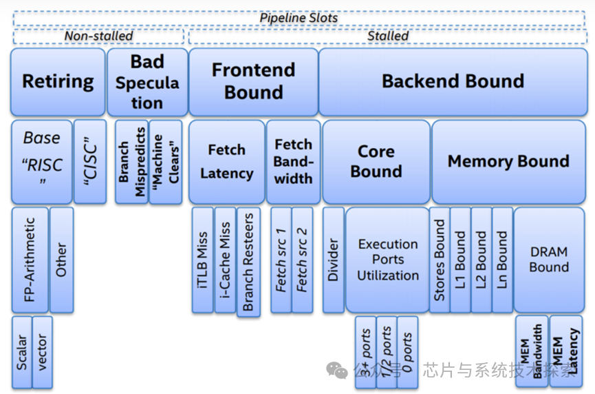
Internally, the CPU can be divided into frontend and backend. The frontend is mainly responsible for fetching values, decoding, etc., and executes sequentially; the backend receives instructions from the frontend and executes them out-of-order, retiring in order. However, due to the high-performance CPUs of today, almost all have branch prediction capabilities. Since it is a prediction, there will inevitably be cases of prediction errors. Therefore, if a CPU experiences a performance bottleneck, it may occur in the frontend or backend, or it may be caused by branch prediction. Thus, in the first level of performance analysis, there are three categories: Frontend, Backend, and Speculation. But why is there also a Retiring category? Here, the Retiring category represents the proportion of ideal pipeline execution.After the first analysis of CPU performance, further second-level and third-level breakdowns are needed.Due to the extensive content, it will be explained in detail as a separate article. If you like this author’s article, please like and follow!