Accurate thermal analysis plays a crucial role in the design of many electronic products, particularly in high-end PCB design. The results of thermal analysis often influence the mechanical layer design of the PCB and the product’s enclosure: whether to install heat sinks, cooling fans, etc. If a cooling fan is installed, it often needs to be quieter, which complicates the mechanical layer design.
The ultimate goal of thermal analysis is to ensure that the entire system can operate stably, especially to ensure that the junction temperature of the chip does not exceed the safe threshold. If this cannot be guaranteed, the FPGA chip will suffer significant drawbacks in performance metrics, reliability, and lifespan, such as continuous system restarts, failure to meet timing requirements, or even failure to ensure correct functionality. Thermal analysis must consider various actual environments in which the FPGA operates: from the ideal environment of a temperature-controlled laboratory to the extreme cold/heat of outer space. The subsequent power consumption analysis is closely related to thermal analysis.
The total power consumption of the entire FPGA design consists of three parts: 1. Static power consumption of the chip; 2. Static power consumption of the design; 3. Dynamic power consumption of the design.
1. Static power consumption of the chip: The power consumed mainly by the leakage current of transistors when the FPGA is powered on but not yet configured.
2. Static power consumption of the design: After the FPGA is configured, when the design has not yet started, it requires maintaining the static current of I/O, clock management, and other circuit static power consumption.
3. Dynamic power consumption of the design: The power consumption of the design after it has started normally; this part of the power consumption mainly depends on the voltage levels used by the chip and the utilization of internal logic and routing resources of the FPGA.
Therefore, the first two parts of power consumption depend on the FPGA chip and hardware design itself, making significant improvements difficult. The third part, dynamic power consumption, can be optimized, and this part accounts for about 90% of the total power consumption. Thus, reducing dynamic power consumption is a key factor in lowering the overall system power consumption.
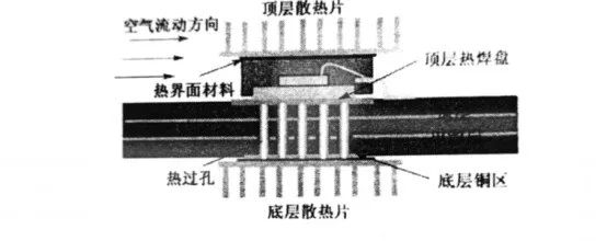
Figure 1 shows the mechanical components that significantly affect the thermal performance of the FPGA chip: heat sinks on the top and bottom layers, pads, and vias. Additionally, the size and quality of the pads, whether thermal grease is used, the extent of air convection, and the size and number of layers of the PCB all influence the final thermal performance metrics.
Static Power Consumption Analysis
 The following formula defines the relationship between ambient temperature, chip junction temperature, power consumption, and thermal resistance: Tj = (θja · Pd) + Ta. Tj represents the junction temperature of the chip, reflecting the maximum temperature that semiconductor devices can withstand; this metric is available in the device manual for each chip. For example, the maximum Tj for the Virtex-6 chip is 125°C, but FPGA tools typically set the default value to 85°C during static timing analysis and power consumption calculations. The junction temperature metrics for different FPGA chips, including their operating ranges, maximum and minimum values, and default values, are detailed in the DC and Switching Characteristics data manual. In the above formula, Ta represents the ambient temperature, and PD represents power consumption. θja is the thermal resistance between the core and the external environment, representing the material’s thermal conductivity, with the physical unit being “°C/W”. The model and parameters shown in Figure 2 are frequently used in various thermal analyses. θjc is the thermal resistance between the core and the package, and the values differ for different devices. For the Virtex-6 package, its typical value is generally less than 0.20 °C/W. θca is the thermal resistance between the package and the external environment, equivalent to the sum of all thermal resistances above the FPGA chip, including heat sinks, cooling fans, thermal grease, and other materials, with the impact of air convection also accounted for. As shown in Figure 2, there are two thermal paths: “core-package-external environment” and “core-PCB-external environment.” Since these two paths are parallel, the total thermal resistance θja can be expressed as θja = (θcA x θjba)/(θjca + θjba), where θjca is the thermal resistance from the top of the package to the external environment, equivalent to θjca = θjc + θca, and θjba is the thermal resistance from the PCB to the external environment, equivalent to θjba = θjb + θba.
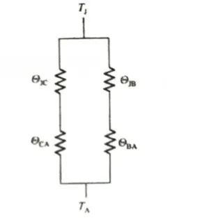 In the modeling process of thermal analysis, the thermal resistance of the PCB itself must also be considered. For small PCBs with fewer layers, the overall θja value is approximately equal to θjca. When θjba is sufficiently large, this component’s contribution to the overall thermal resistance becomes very small and can even be ignored. The larger the PCB and the more layers it has, the larger the corresponding θjba value. Table 1 illustrates the impact of PCB size and layer count on thermal performance.
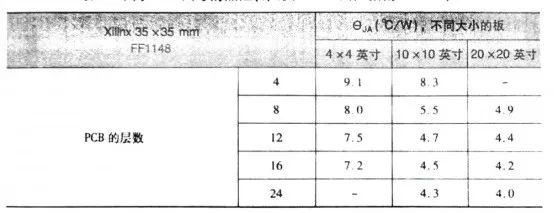 For the entire thermal analysis, the most important aspect is to correctly establish the thermal model. As shown in Table 2, if the thermal resistance of the PCB is not considered, the final result will be extremely inaccurate.
Static Power Dissipation Methods
Air Cooling
For low-end, small-package FPGA chips with a power dissipation of about 1-6W, air convection or the addition of heat sinks is generally sufficient for cooling. The role of the heat sink is to quickly dissipate heat from the chip surface, so high thermal conductivity metals like aluminum or copper are typically used as heat sink materials. Heat sinks usually have a large surface area, allowing for faster heat dissipation. The contact area between the heat sink and the chip is crucial for heat dissipation; therefore, using thermal grease to tightly connect the heat sink and the chip surface can further accelerate heat conduction. In a good air convection environment, for chips with power dissipation around 4-10W, using heat sinks is an excellent choice.
Active Cooling
For chips with power dissipation between 8-25W and using large packages, a combination of heat sinks and fans can achieve better cooling effects. For example, given the junction temperature and ambient temperature, the maximum allowable power dissipation can be calculated: Tj = +85°C, Ta = +55°C, and the device is a Virtex-6 chip, with thermal resistance θjc = 0.20°C/W. The thermal resistances of the heat sink and fan are: θca = 1.80°C/W, θjb = 0.40°C/W, and θba = 2.60°C/W. By iterating through the following formulas, the power dissipation PD can be calculated: Tj = (θja x Od) + Ta, θja = (θca x θjba)/(θjca + θjba), θjca = θjc + θca = 0.2 + 1.8 = 2.0°C/W, θjba = θjb + θba = 0.4 + 2.6 = 3.0°C/W, θja = (2.0 x 3.0)/(2.0 + 3.0) = 1.2°C/W, PD = (Tj – Ta)/θja = (85 – 55)/1.2 = 25W. From the above formulas, it can be seen that under the given conditions of chip junction temperature, ambient temperature, and thermal resistance, the total power dissipation of the FPGA chip will not exceed 25W.
Dynamic Power Consumption Optimization Methods
Algorithm Optimization
Algorithm optimization can be explained at two levels: implementation structure and implementation method. First, it is essential to design an optimized algorithm implementation structure that minimizes resource usage while also reducing power consumption, but performance must also be guaranteed, allowing FPGA design to balance area and speed. For example, when choosing between a pipeline structure and a state machine structure, the pipeline structure has all states working simultaneously, while the state machine structure has only one state enabled. It is evident that the pipeline structure consumes more power, but it offers better data throughput and system performance; thus, a reasonable choice must be made to balance area and speed. The second level concerns specific implementation methods; among all signals that consume power in the design, the clock is the main culprit. Although the clock may operate at 100MHz, the signals derived from that clock typically operate at a smaller fraction of the main clock frequency (usually 12%-15%). Additionally, the clock’s fanout is generally high. These two factors indicate that to reduce power consumption, careful consideration of the clock is necessary. First, if a certain part of the design can be inactive, consider disabling the clock tree flip instead of using clock enable. Clock enable prevents unnecessary flips of registers, but the clock tree will still flip, consuming power. Second, isolate the clock to use the minimum number of signal regions. Unused clock tree signal regions will not flip, thereby reducing the load on the clock network.
Resource Utilization Efficiency Optimization
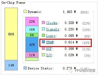
Resource utilization efficiency optimization introduces methods to optimize power consumption when using internal FPGA resources such as BRAM and DSP48E1. The dynamic power consumption of FPGAs mainly manifests in the power consumed by memory, internal logic, clocks, and I/O. Among these, memory is a significant power consumer, such as the Block RAM in Xilinx FPGAs. Therefore, this section mainly introduces some power optimization methods for BRAM. As shown in Figure 5, although BRAM only uses 7%, its power consumption of 0.601W accounts for 42% of the total design, so optimizing BRAM power consumption can effectively reduce the dynamic power consumption of the FPGA.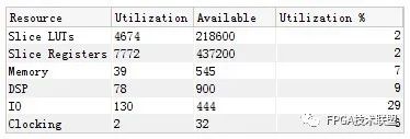
 The following methods for optimizing BRAM power consumption are introduced: a) Use “NO CHANGE” mode: When BRAM is configured as True Dual Port, it is necessary to select the operation mode of the ports: “Write First,” “Read First,” or “NO CHANGE” to avoid conflicts between read and write operations, as shown in Figure 6. The “NO CHANGE” mode indicates that BRAM does not add extra logic to prevent read/write conflicts, thus reducing power consumption, but the designer must ensure that no read/write conflicts occur during program execution.
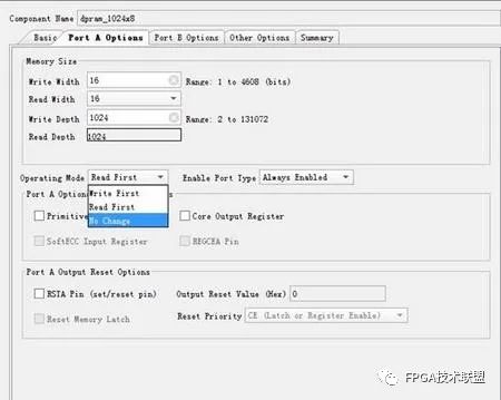 The power consumption in Figure 5 is set to “Write First,” while Figure 7 shows the power consumption after setting to “NO CHANGE,” where BRAM power consumption decreased from 0.614W to 0.599W. If a large amount of BRAM is used in the design, the effect will be more pronounced.
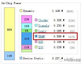 Figure 7 b) Control the “EN” signal: The BRAM ports have a clock enable signal, as shown in Figure 8. In the port settings, this can be enabled, and when the module is instantiated, it can be connected to the read/write signals. This optimization allows BRAM to stop working when there are no read/write operations, saving unnecessary power consumption.
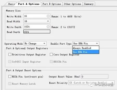 Figure 8 shows the power consumption after controlling the “EN” signal, where BRAM power consumption decreased to 0.589W.
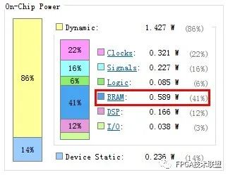 Figure 9 c) Depth Concatenation: When a large amount of memory is used in the design, multiple BRAMs need to be concatenated. For example, if a depth of 32K and a width of 32-bit are required, how to configure a single BRAM of 32K32Bit storage is a question. In 7 series FPGAs, the BRAM is 36Kb, where 32Kb capacity is generally used, so it can be configured as 32K1-bit or 1K*32-bit. When concatenating multiple BRAMs, the former is “width concatenation” (see Figure 10), and the latter is “depth concatenation” (see Figure 11). In both structures, the “width concatenation” structure requires all BRAMs to perform read/write operations simultaneously, while the “depth concatenation” structure only requires one BRAM to perform read/write operations. Therefore, in low power consumption scenarios, the “depth concatenation” structure is preferred. Note: The “depth concatenation” structure requires additional data selection logic, increasing the number of logic layers, sacrificing area and performance to reduce power consumption.
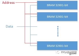 Figure 10
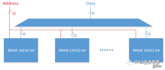 Figure 11References[1] Xilinx XPower Estimator (XPE) tool for performing thermal and power analysis http://www.xilinx.com/products/design_resources/power_central [2] Considerations for heatsink selection, Xilinx White Paper WP258 www.xilinx.com/support/documentation/white_papers/wp258.pdf [3] Virtex-6 Packaging and Pinout Specifications, Xilinx User Guide UG365 www.xilinx.com/support/documentation/user_guides/ug365.pdf [4] National Semiconductor Application Note 2026 www.national.com/an/AN/AN-2026.pdf
For more interesting topics, please see the links:
FPGA Knowledge Collection – What tasks are included in FPGA project development?
FPGA Knowledge Collection – FPGA Structure (1)
Applications of FPGA
FPGA Knowledge Collection – Using Xilinx tools in command line mode
FPGA Knowledge Collection – Useful tools in ISE you should know?
FPGA Knowledge Collection – What EDA tools should you be familiar with for FPGA design development?
FPGA Knowledge Collection – FPGA code naming conventions worth collecting?
FPGA Knowledge Collection – Setting environment variables for ISE under Linux
FPGA Knowledge Collection – Verilog coding styles worth collecting 1
FPGA Knowledge Collection – Verilog coding styles worth collecting 2
FPGA Knowledge Collection – Summary of rules to pay attention to when writing synthesizable code (RTL)
FPGA Knowledge Collection – Mixed use of Verilog and VHDL
FPGA Knowledge Collection – About Xilinx tool reports
FPGA Knowledge Collection – Instantiation and synthesis
Hardware simulation accelerators and prototype verification platforms
FPGA Knowledge Collection – Porting from ASIC to FPGA
FPGA Knowledge Collection – Porting clock systems