In the early stages of IC design, the main parameters of concern were performance (timing) and area. EDA tools minimized area while meeting performance requirements. At this time, power consumption was not a major concern.
Because CMOS technology exhibits relatively low power consumption at lower clock frequencies, leakage current can be negligible. However, as transistor density and clock frequency increase, the static power consumption of CMOS technology also rises significantly. Meanwhile, reductions in supply voltage and threshold voltage lead to increased leakage current.
These factors make power consumption a key parameter affecting performance and area, making power consumption issues as critical as performance/area.
Problems Caused by High Power Consumption
Excessive power consumption can have various negative impacts.
-
It leads to increased chip temperature, necessitating more expensive ceramic packaging and cooling systems.
-
High temperatures can reduce the reliability and lifespan of the chip.
-
It shortens the battery life of portable devices. As functionality increases, battery technology has not kept pace with power consumption demands.
-
It increases the power supply costs and environmental burden of widely used electronic devices. Even minor reductions in power consumption can save users significant costs and resources.
Dynamic Power and Static Power
IC design must consider dynamic power and static power.
-
Dynamic power is the power consumed when transistors switch, related to clock frequency and switching activity.
-
Static power is the power consumed due to transistor leakage current, independent of clock frequency or switching activity.
Dynamic power consists of switching power and short-circuit power. Switching power is the power consumed when charging and discharging the circuit’s load capacitance. Short-circuit power is the power consumed by the short-circuit current flowing through PMOS and NMOS during logic state transitions. The following figure illustrates the reasons for switching power.
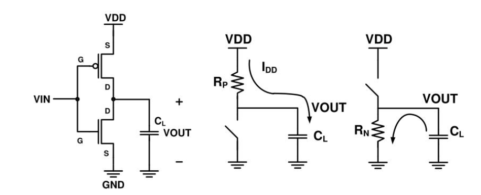
When the inverter output changes from 0 to 1, the PMOS charges the load capacitance; when it changes from 1 to 0, the NMOS discharges the load capacitance. Thus, dynamic power is related to supply voltage, load capacitance, clock frequency, and switching activity.
In early CMOS technology, leakage current was minimal. However, as transistor size and threshold voltage decrease, leakage power increases, sometimes reaching levels comparable to dynamic power. Leakage current occurs whenever power is supplied to the transistor. Slowing down or stopping the clock does not reduce leakage power; only lowering or shutting off the supply voltage can reduce or eliminate leakage power.
Low-Power Design Methods
Reducing power consumption is a crucial objective in digital IC design. To achieve this, different design strategies can be employed at the RTL level and gate level. Clock gating is a commonly used method that stops the clock signal to registers when they remain unchanged, thereby reducing dynamic power consumption. Other methods, such as dynamic voltage and frequency scaling, while capable of adjusting voltage and frequency according to workload, are more challenging to implement.
As process technology advances, power consumption issues become increasingly prominent, necessitating the development of more methods to meet design power requirements.
1. Lowering Supply Voltage
Lowering supply voltage is one of the most fundamental methods to reduce power consumption, as power consumption is proportional to the square of the supply voltage, as shown in the figure.
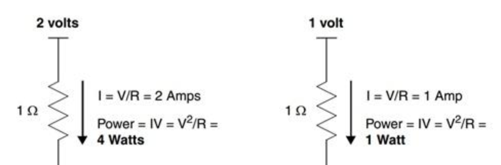
If the supply voltage is reduced by 50%, power consumption can be reduced by 75%. CMOS technology has continuously lowered supply voltage to reduce power consumption, starting from 5V supply in bipolar TTL circuits in the 1980s to about 1V in current advanced processes. However, lowering supply voltage also affects switching speed and noise immunity, and increases leakage current and interface complexity.
2. Clock Gating
Clock gating is an effective method to reduce dynamic power consumption, allowing the clock signal to be stopped when registers maintain the same logic value, thus avoiding unnecessary switching activity. The implementation of clock gating is illustrated in the figure:
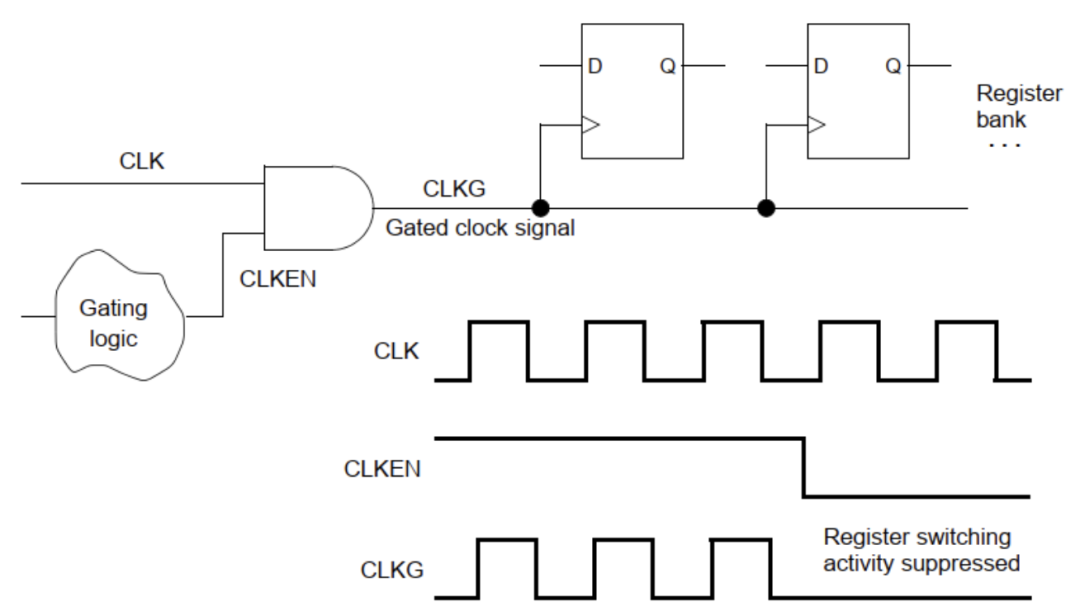
Clock gating is suitable for registers that need to maintain the same logic value across multiple clock cycles. Disabling the clock can save the power consumed by re-triggering the register in each clock cycle. The main challenge of clock gating is finding suitable locations and generating clock gating signals at the right time. Clock gating is a mature power reduction technique that has been widely used for many years. Tools like Power Compiler can automatically insert clock gating cells in clock paths. Clock gating is relatively simple to implement, as it only requires modifying the netlist.
3. Multi-Threshold Standard Cell Libraries
Some CMOS standard cell process libraries offer standard cells with different threshold voltages (Vt). This allows the standard cell library to provide standard cells with varying threshold voltages to achieve the same logic function. For example, the library can provide two inverter cells: one using low-threshold (Low-Vt) transistors and the other using high-threshold (High-Vt) transistors.
-
Low-threshold cells have higher speed and larger leakage current.
-
High-threshold cells have smaller leakage current but slower speed.
Synthesis tools can select the appropriate type of standard cell based on the trade-off between speed and power consumption.
For instance, it can use low-threshold cells on critical paths and high-threshold cells on non-critical paths.
4. Multi-Voltage Design
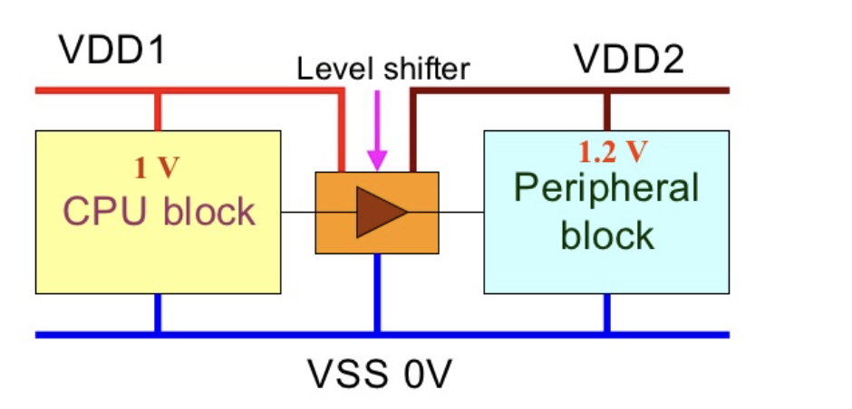
Different parts of a chip may have different speed requirements. For example, the CPU and RAM modules may need to operate faster than peripheral modules. As mentioned earlier, lower supply voltage can reduce power consumption but also decreases speed, as shown in the figure.
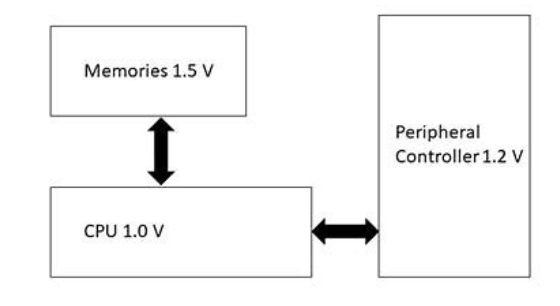
Providing two or more supply voltages on a single chip introduces some complexity, and the power grid must separately allocate each voltage source to the appropriate module. If a logic signal crosses from one voltage domain to another, a level-shifter unit is needed to produce a signal with the appropriate voltage swing. In the example shown in the above figure, the level shifter converts a 1.0V signal to a 1.5V signal. The level shifter itself requires two power supplies that match the input and output supply voltages.
5. Power Switches
Power switches are a technique to reduce power consumption by cutting off power to parts of the chip that do not need to operate.
For instance, in mobile phone chips, the voice processing module can be powered down when the phone is in standby mode. When a user makes or receives a call, the voice processing module must be “woken up” from the powered-down state.
Power switches can significantly reduce overall power consumption, as they reduce both static and dynamic power. However, they also introduce other challenges, including the need for power control, power switch networks, isolation cells, and retention registers.
Power control is a logic block that determines when to cut off and restore power. Turning power on and off requires time and power costs, so the power controller should determine the appropriate power-off timing. Modules that can be powered down must be connected to a power switch network consisting of a large number of series transistors between the always-on power rail and the power pins. The power switch network is distributed around or within the module.
-
When turned on, it connects the power to the logic gates within the module.
-
When turned off, it disconnects the logic gates in the module from the power.
Using high-threshold transistors from multi-threshold CMOS (MTCMOS) technology as power switches is beneficial because they minimize leakage power, and their switching speed is not critically important. PMOS switches can be placed between VDD and the module’s power pins, while NMOS switches can be placed between VSS and the module’s ground pins, as shown in the figure.
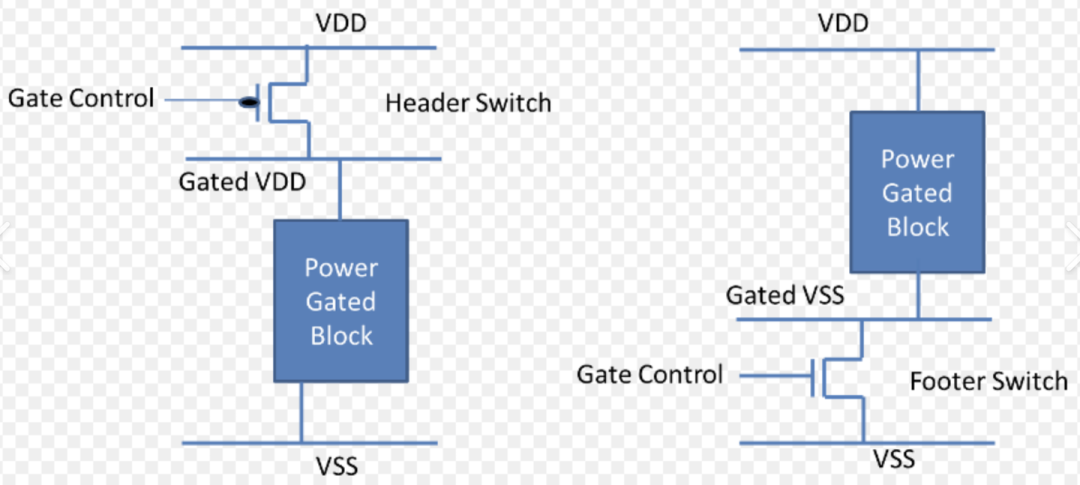
It is essential to reasonably select the number, drive strength, and location of switches to ensure acceptable voltage drop (IR Drop) during module operation.
The power switch strategy shown in the above figure is called coarse-grained strategy, as the entire module shares one or more parallel power switches. In fine-grained strategy, each library cell has its independent power switch. Fine-grained strategy can further reduce power consumption but also requires more area.
When signals transmit from powered-down modules to always-on modules, isolation cells are needed. Isolation cells can provide a fixed logic value to always-on modules when powered-down modules are off, thereby avoiding potential leakage current. A simple implementation of isolation cells is illustrated in the figure.
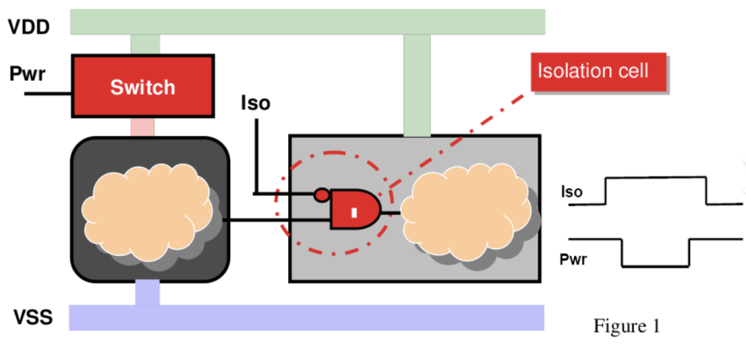
When the left module is powered on, the Iso signal is low, and the output signal remains unchanged through the isolation cell (except for delay). When the left module is powered down, Iso is high, and the output signal maintains a constant logic 0. Other types of isolation cells can maintain logic 1 or the signal value before power-off. During the powered-down period, the isolation cell itself must have an always-on power supply.
Power switches can be combined with multi-voltage techniques. Different modules can operate at different voltages and can also be powered down separately. In such cases, the interface units between different modules must simultaneously incorporate level-shifting and isolation functions. This type of unit is called an enable level shifter. This unit must have two independent power supplies, just like a standard level shifter.
When a module is powered down and then powered back on, it typically needs to return to its state before power-off. Several methods can achieve this goal. For example, the contents of the registers within the module can be copied to external RAM before power-off and then copied back after power-on.
Another method is to use retention registers within the powered-down module. Before power-off, retention registers can save data to shadow registers, retaining data during power-off. After power-on, they can restore data from shadow registers back to the main registers. Shadow registers have an always-on power supply but use high-threshold transistors to minimize leakage power during power-off. The main registers use fast but leaky low-threshold transistors. An implementation of retention registers is illustrated in the figure.
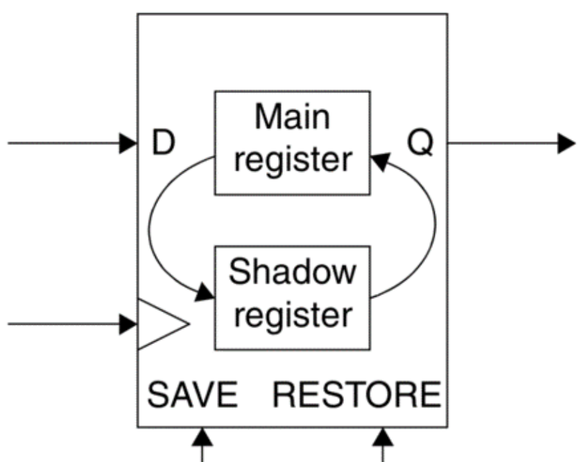
The SAVE signal saves register data to shadow registers before power-off and the RESTORE signal restores data after power-on. Retention registers use level-sensitive control signals instead of edge-sensitive SAVE and RESTORE signals.
Retention registers occupy more area than normal registers and require an always-on power supply in addition to the power used by the rest of the module.
6. Dynamic Voltage and Frequency Scaling
Building on multi-voltage techniques, voltage and frequency can be dynamically adjusted based on the real-time workload of the chip, optimizing power consumption. For example, in laptops, the processor chip can use lower voltage and frequency during simple spreadsheet calculations to save power; while higher voltage and frequency can be used during 3-D image rendering to enhance performance. This technique of varying supply voltage and operating frequency according to workload requirements is called dynamic voltage and frequency scaling.
Chip power supplies can be designed to have multiple discrete or continuous voltage levels. Dynamic voltage scaling requires multi-level power supplies and logic modules to determine the optimal voltage level for a given task.
Due to the existence of multiple possible voltage and frequency combinations, design, implementation, verification, and testing are very challenging.
Dynamic voltage scaling can be combined with power switch technology. Modules in the design can operate at different voltage levels to meet different performance requirements or be completely powered down when not in use.