CMOS Characteristics
The essence of a CMOS Sensor is a linear sensor that measures photoelectric conversion events, which can be considered a photon counter to some extent. The reading value of each pixel on the Sensor reflects the number of photons captured by that pixel within a specified time. An ideal Sensor should possess the following characteristics:
a) The output is directly proportional to the input (no Sensor noise, only the noise of the signal itself);
b) Both input and output can be infinitely large;
c) High sensitivity, small input generates large output;
d) High frame rate;
e) High resolution;
f) Low power consumption;
g) Simple process;
h) Low cost.
The response characteristics of an ideal CMOS Sensor are shown in the figure below.
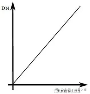
The slope of the straight line in the figure below determines the size of the response that can be excited by a unit input, and this slope is called the gain coefficient (Gain). The Sensor will provide a set of interfaces to adjust the actual effective gain value.
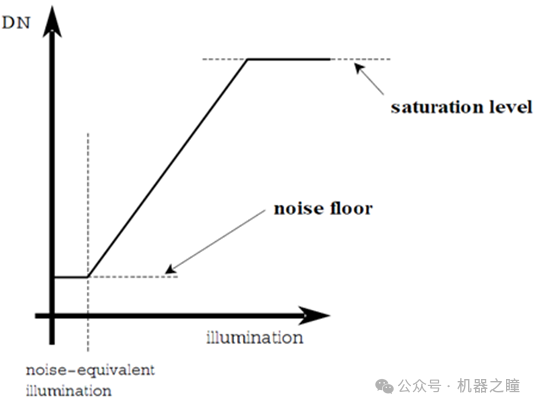
However, the actual Sensor can only maintain linear response within a limited range, and cannot accurately represent input signals that are too small or too large, as shown in the figure below.
CMOS Noise (Noise)
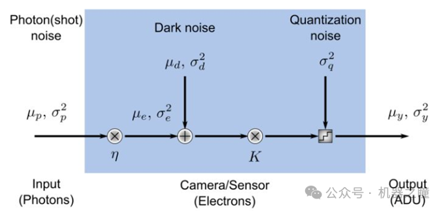
Assuming constant and uniform illumination intensity, the noise in the image captured by the camera is the sum of spatial and temporal fluctuations in the measured signal. The figure below summarizes the CMOS photoelectric conversion model and the mathematical models of several main noise types in the form of a transfer function.
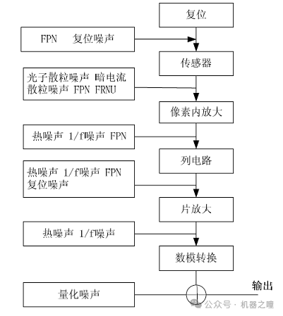
The figure below describes in more detail the sources and locations of various noises during the imaging process of the CMOS.
1. Dark Current Noise (Dark Noise)
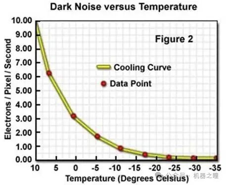
The thermal motion of electrons in the silicon wafer can lead to some valence electrons being randomly excited to the conduction band, forming dark current (Dark Current), so even in the absence of photons, the Sensor will still have a certain signal output. During exposure, the random variation of dark current forms dark shot noise. The main reason for the variation in dark current is that electrons encounter the potential barrier of the PN junction when passing through it (Darrier), and electrons need to undergo a process of kinetic energy – potential energy – kinetic energy conversion to cross the barrier, which takes some time. Dark shot noise statistically follows a Poisson distribution, independent of the level of light signals but related to the temperature of the sensor. The general rule is that for every 8°C increase in temperature, the dark current doubles. Therefore, when designing circuits, it is essential to place heat-generating electronic components as far away from the Sensor as possible.
2. Readout Noise
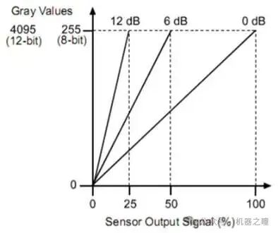
This noise is generated during the production of electronic signals.The Sensor uses an AD converter (ADC) to sample the analog voltage output from the analog amplifier into a digital voltage. Since the precision of digital signals is always limited, typically between 10 bits to 14 bits, the analog signal that falls between two adjacent digital values will be rounded to the nearest value, introducing quantization noise, which is a significant component of readout noise. This noise is determined by the design of the sensor, indicating the minimum number of electrons required to drive the readout circuit’s ADC to change one bit. It is independent of the signal level and the temperature of the sensor.
3. Shot Noise (Shot Noise)
This noise is statistical noise related to the photons falling on the sensor pixels. At the microscopic scale, the behavior of photon flow reaching the sensor is uneven in time and space, similar to the flow of cars on a busy highway, sometimes dense and sometimes sparse. Sometimes the left lane is dense, and after a while, the right lane becomes dense, overall following a statistical pattern that conforms to a Poisson distribution. Photon shot noise is related to the level of the measured signal and is independent of the temperature of the sensor.
4. Fixed Pattern Noise (FPN)
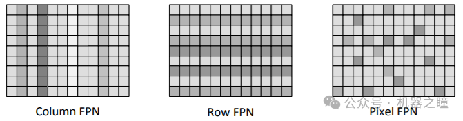
This noise is caused by the spatial non-uniformity of the pixels. Each pixel in the CMOS is equipped with a charge voltage amplifier, and there are some transistors in each row and column to control the reset and readout of the pixels. The drift of these devices’ working parameters relative to theoretical values constitutes a type of fixed pattern noise. Additionally, defective or bad pixels can also be considered a type of fixed pattern noise, which can be roughly simulated by the diagram below.
5. Reset Noise
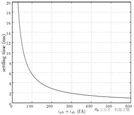
The rolling shutter exposure method requires resetting the potential well first, releasing all the charge accumulated in the potential well to prepare for subsequent readout. However, due to the presence of dark current, some random noise signals of varying sizes will remain after each reset, known as reset noise, which is related to the pixel structure, chip temperature, and PN junction capacitance, hence also referred to as kTC noise. Resetting the pixel takes a certain amount of time. Quantitative studies show that even with a larger reset current, it generally takes more than 1ms to cleanly release the charge, as shown in the figure below.
The actual reset control signal is usually shorter than 1ms, so the next frame image will somewhat retain some shadow of the previous frame, known as Image Lag, which is also a form of noise.
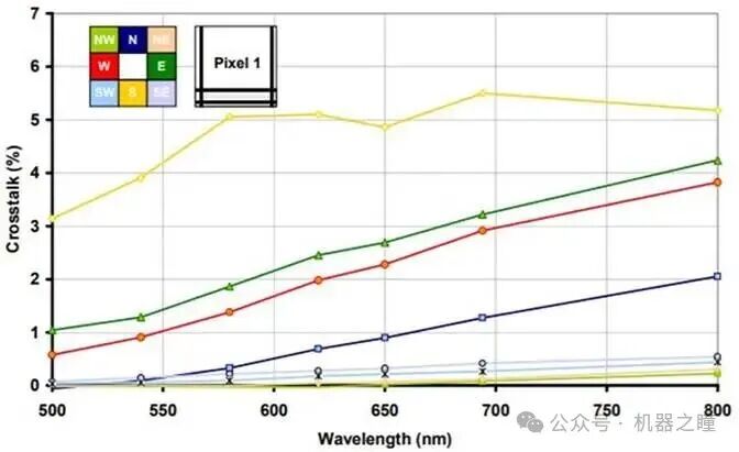
6. Crosstalk Noise (Crosstalk)
In the communication field, it refers to signal coupling between two signal lines due to poor shielding, where a signal on one line is fed into a nearby signal line through mutual inductance and capacitance. In the analog communication era, this could lead to overhearing someone else’s conversation. In the Sensor field, crosstalk refers to the incident light signal on one pixel A not being captured in that pixel but instead being captured by surrounding pixels B, resulting in B producing an unintended signal.
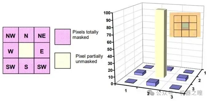
In the example below, the pink represents opaque pixels that should not have any output, while the yellow represents normal pixels that should have output. In reality, photons can penetrate a certain distance in the silicon wafer, allowing them to enter the photosensitive area of the pink pixels, thus generating a signal for the pink pixels, which is the crosstalk mechanism of CMOS.
As shown in the figure below, the longer the wavelength, the more severe the crosstalk, with crosstalk energy at certain pixel locations reaching up to 5%.