Click the blue text to follow us
Research Background
The emerging photoelectrochemical (PEC) photodetectors possess unique characteristics for operation in liquid environments. Unlike electrochemical methods that require an external power source to generate electrical detection signals, PEC photodetectors separate the electrical detection signal from the light excitation source, resulting in negligible background signals and reduced interference from active substances. These features make PEC photodetectors an ideal sensor architecture for biosensing applications, allowing for easier integration and compatibility with biological systems. Meanwhile, during the exploration of efficient biosensors, responsiveness and stability are key characteristics that directly affect their sensing performance in various application scenarios. However, achieving high responsiveness and stability in PEC photodetectors to ensure optimal sensing performance remains a challenge. Essentially, the performance of PEC photodetectors depends on three different carrier transport characteristics: (1) within the semiconductor, (2) at the semiconductor/electrolyte interface, and (3) in surface chemical reactions. This unique operational characteristic, based on the coupling of internal and external carrier transport with surface reactions, presents new opportunities for us to achieve high-performance PEC biosensors by adjusting and optimizing their physical and chemical processes.
 Facile Semiconductor p–n Homojunction Nanowires with Strategic p-Type Doping Engineering Combined with Surface Reconstruction for Biosensing ApplicationsLiuan Li, Shi Fang, Wei Chen, Yueyue Li, Mohammad Fazel Vafadar, Danhao Wang, Yang Kang, Xin Liu, Yuanmin Luo, Kun Liang, Yiping Dang, Lei Zhao, Songrui Zhao, Zongzhi Yin & Haiding SunNano-Micro Letters (2024)16: 192
https://doi.org/10.1007/s40820-024-01394-5
Highlights of the Article
1. Excellent photoelectrochemical sensing performance: The designed PEC photodetector composed of GaN nanowires exhibits a high responsiveness of 247.8 mA W⁻¹ and ultra-stable operational characteristics.
2. Internal + external energy band engineering of semiconductor nanowires: Facilitating effective PEC reactions by controlling carrier dynamics while protecting the nanowires from photo-corrosion.
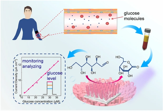
3. Construction of a glucose sensing system: Successfully analyzed blood glucose levels in human serum samples, demonstrating a high sensitivity of 0.173 μA μM⁻¹ cm⁻² and a low detection limit of 0.07 μM..
Content Summary
Professor Haiding Sun from the University of Science and Technology of China, in collaboration with Professor Zongzhi Yin’s team from Anhui Medical University, and Professors Yiping Dang and Lei Zhao from Tongji Medical College, Huazhong University of Science and Technology, constructed a p-n homojunction nanowire structure based on GaN and strategically doped the p-GaN segment, while modifying the surface of the nanowires with cobalt nickel oxide (CoNiOₓ), designing and fabricating a novel PEC photochemical sensor based on semiconductor p-n junctions. Under illumination, the p-n homojunction acts as a “hole pump,” effectively transferring photogenerated holes to the surface of the nanowires. Compared to pure n-GaN nanowires, the photovoltage of the p-n homojunction nanowires increased by 172%, significantly improving the internal carrier separation efficiency. Additionally, through targeted doping of the p-GaN segment, the hole transfer barrier at the p-GaN/electrolyte interface was minimized, facilitating the migration of photogenerated holes into the electrolyte. Furthermore, to further enhance the carrier migration process, CoNiOₓ was used for surface modification, forming a p-n GaN/CoNiOₓ structure. The device achieved a high responsiveness of 247.8 mA W⁻¹ while exhibiting excellent operational stability, showing negligible attenuation during a 27.5-hour stability test. Ultimately, due to its remarkable stability and high responsiveness, as well as its unique operation in aqueous environments, we successfully constructed a glucose sensing system with high linear response and selectivity, successfully detecting blood glucose levels in human serum samples. This research provides a simple and universal route to unleash the full potential of PEC devices in future advanced biosensing applications.
Illustrated Guide
I Energy Band Structure Design of GaN Nanowires
The structure of GaN nanowires was designed to construct a p-n homojunction. Figure 1a shows the n-GaN nanowire, and Figure 1b shows the schematic structure of the p-n GaN nanowire. Figure 1c presents the energy band diagram of the n-GaN nanowire, while Figure 1d shows the energy band diagram of the p-n GaN nanowire. The photovoltage characterization of n-GaN and p-n GaN nanowires (Figure 1e) demonstrates that the presence of the p-n homojunction significantly enhances the internal carrier separation efficiency of the nanowires. Figure 1f illustrates the relationship between the surface energy band bending of the p-GaN segment and the photocurrent, indicating that smaller surface energy band bending corresponds to effective hole transport, leading to larger photocurrent responses.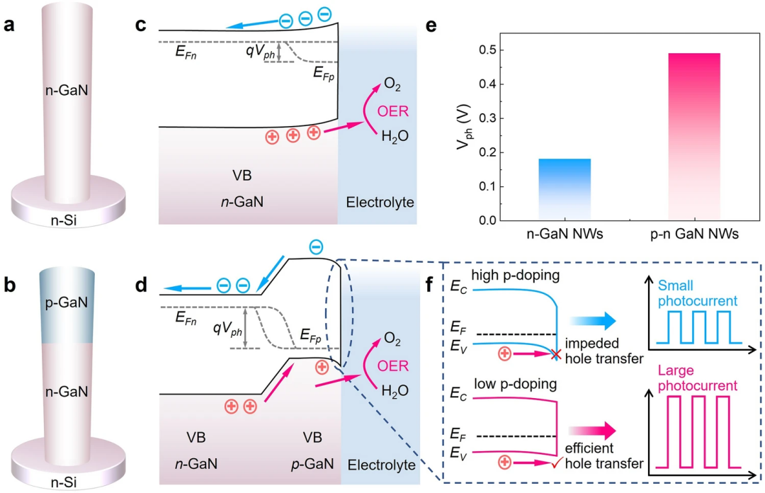 Figure 1. Energy band structure design of GaN nanowires. (a) Schematic structure of n-GaN and (b) p-n GaN nanowires; energy band diagrams of (c) GaN and (d) p-n GaN nanowires in contact with the electrolyte under illumination. EFn and EFp are the quasi-Fermi levels for electrons and holes, respectively. Vph represents the photovoltage generated in the nanowires; (e) Comparison of photovoltage between n-GaN and p-n GaN nanowires; (f) Relationship between surface energy band bending of the p-GaN segment and photocurrent.
II Charge Transfer Characteristics Study and Surface Energy Band Characterization
To investigate the doping situation in p-n GaN nanowires, characterization was performed using Mott-Schottky (M-S) (Figure 2a), Kelvin Probe Force Microscopy (KPFM) (Figure 2b), and X-ray Photoelectron Spectroscopy (XPS) (Figure 2b), confirming the successful preparation of p-n GaN nanowires with three different doping concentrations. The electrochemical impedance spectroscopy (EIS) was characterized under 340 nm illumination (Figure 2c), and the fitted values of charge transfer resistance (Rct), bulk resistance (Rbulk), and solution resistance (Rs) were extracted from the EIS plot (Figure 2d), confirming that the hole transport barrier under low doping conditions is minimal. Photoreponse tests were conducted on p-n GaN nanowires with different doping concentrations (Figure 2e), showing that the photoreponse performance of the low-doping sample is the best. The internal carrier transport performance of the nanowires was directly characterized using KPFM (Figure 2f), confirming that the low-doping p-n GaN nanowires have the highest internal carrier separation efficiency, corresponding to the photoreponse performance.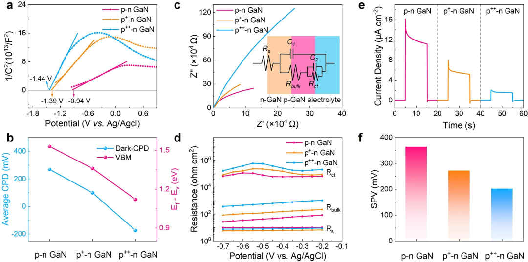 Figure 2. Charge transfer characteristics study and surface energy band characterization. (a) M-S measured under dark conditions; (b) Contact potential difference (CPD) measured with KPFM, XPS valence band spectrum showing the position of the valence band top relative to the Fermi level; (c) EIS spectrum measured under 340 nm light, light intensity of 0.1 mW cm⁻² (0 V vs. Ag/AgCl); (d) Extracted fitting values of Rct, Rbulk, and Rs (measured at different bias voltages); (e) Measured photocurrent under 340 nm light, light intensity of 0.1 mW cm⁻²; (f) Surface photovoltage (SPV) measured with KPFM under 340 nm light.II Surface Modification and Material CharacterizationThe original GaN surface has surface states and various defects that limit the rapid migration of photogenerated carriers. Additionally, the lack of reactive active sites on the original GaN surface restricts the rate of surface chemical reactions, causing carriers to accumulate on the surface of the nanowires, which affects device performance (Figure 2a). To accelerate the consumption of photogenerated carriers and improve the long-term stability of the device, surface modification of GaN nanowires is necessary. CoNiOₓ is a bimetallic oxide commonly used as a hole transport layer and as an efficient co-catalyst for the oxygen evolution reaction, effectively enhancing carrier extraction efficiency. Therefore, CoNiOₓ was used as a co-catalyst for surface modification of p-n GaN. Scanning Electron Microscopy (SEM) images show the morphology of the modified nanowires (Figure 2b). Transmission Electron Microscopy (TEM) images (Figure 2c) and High-Resolution Transmission Electron Microscopy (HRTEM) images (Figure 2d) reveal that the surface of the modified nanowires has a layer of amorphous material. EDS elemental mapping (Figure 2e) and Co (Figure 2f), Ni (Figure 2g) XPS spectra show the elemental distribution on the nanowires, confirming the successful modification of CoNiOₓ.
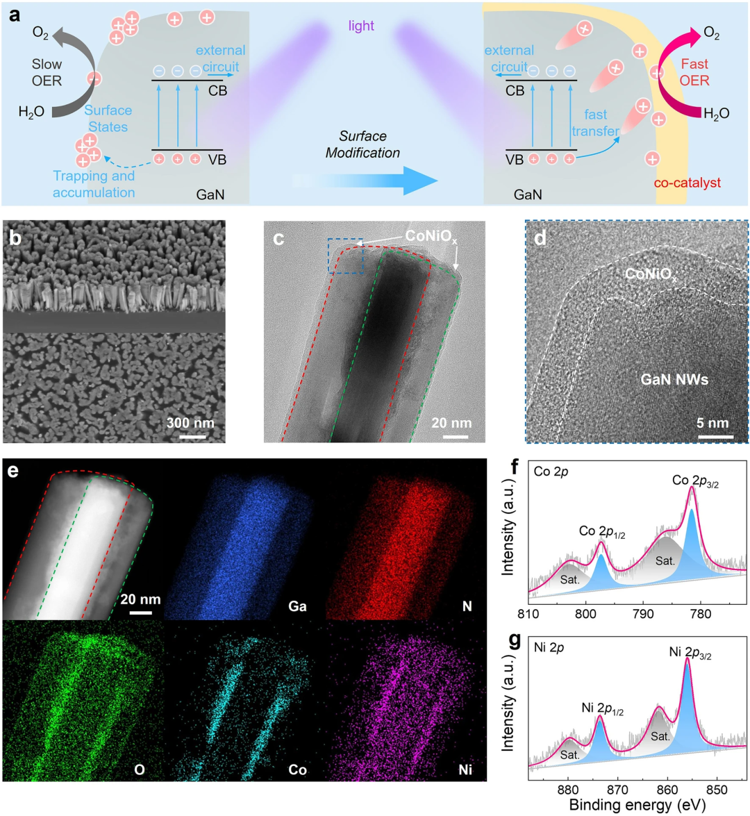 Figure 3. Surface modification and material characterization. (a) Schematic diagram of carrier dynamics of original GaN and surface-modified GaN nanowires; (b) SEM images of p-n GaN/CoNiOₓ nanowires at a 30° tilt and top view; (c) TEM images of p-n GaN/CoNiOₓ nanowires; (d) Magnified image of the blue outlined area in (c); (e) EDS elemental mapping of p-n GaN/CoNiOₓ nanowires. XPS spectra of (f) Co and (g) Ni on p-n GaN/CoNiOₓ nanowires.
IV Study of Photogenerated Carrier Dynamics and Photoreponse Characteristics Testing and Analysis
Photogenerated carrier dynamics studies were conducted on the modified p-n GaN/CoNiOₓ nanowires. First, time-resolved photoluminescence (TRPL) (Figure 4a) was used to characterize the carrier lifetime before and after modification, indicating that the carrier lifetime of the nanowires is longer after CoNiOₓ modification. Further tests of open-circuit potential (OCP) (Figure 4b) and KPFM (Figure 4c) photovoltage showed that CoNiOₓ modification effectively suppressed the surface states of the nanowires, shielding the carrier trapping effect and significantly enhancing carrier migration. Subsequently, the photoreponse performance of the nanowires was characterized. Through I-t testing (Figure 4d) and spectral response testing (Figure 4e), it was shown that the p-n GaN/CoNiOₓ exhibited a 101.6% improvement in responsiveness compared to p-n GaN. Tests under different light intensities demonstrated good linear response (Figure 4f). Finally, long-term I-t testing was conducted, showing negligible attenuation of photocurrent after a 27.5-hour test (Figure 4g), demonstrating excellent operational stability. Figure 4h compares the performance of this work with other similar self-powered photodetectors, showcasing the superior performance, responsiveness, and stability of this work.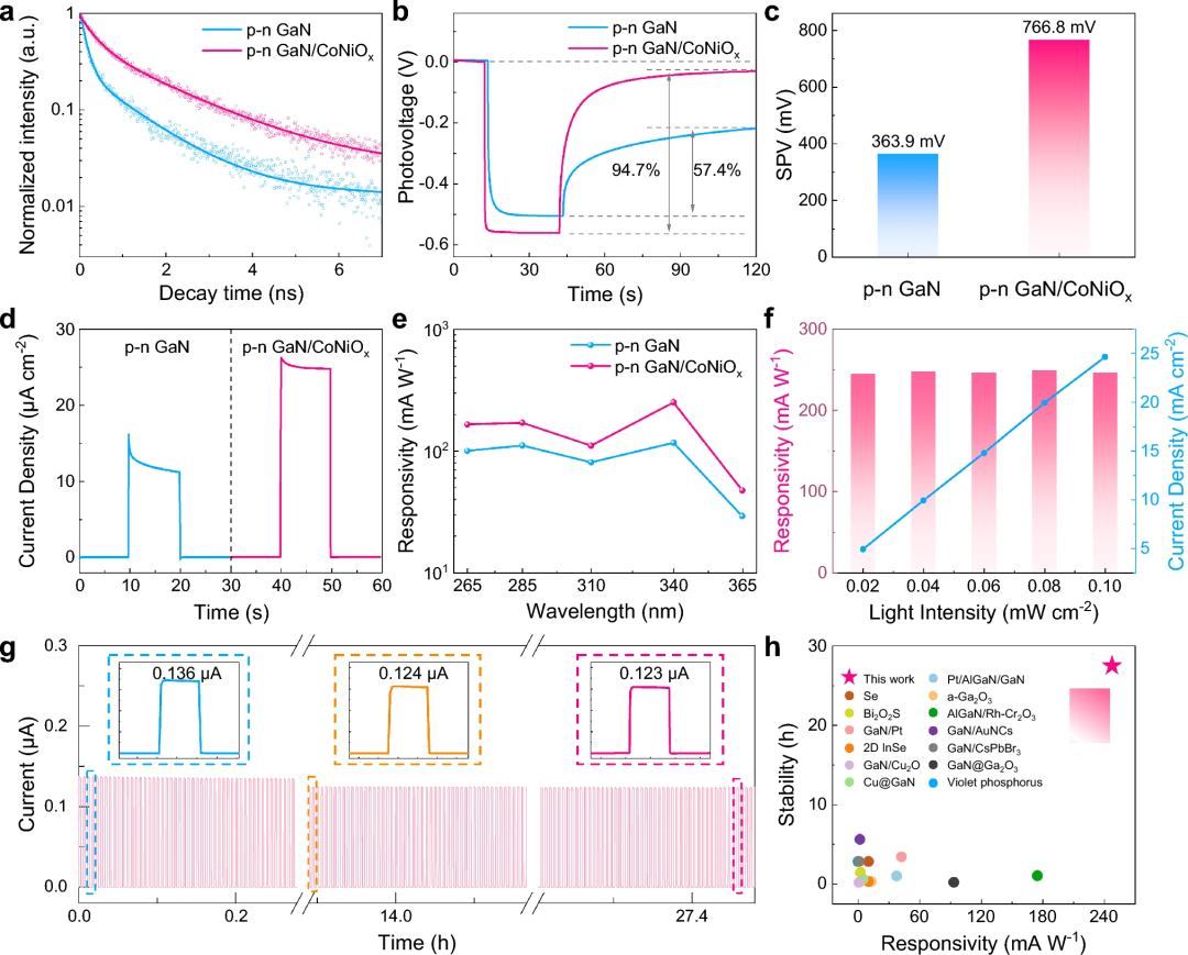
Figure 4. Study of photogenerated carrier dynamics and evaluation of photoreponse. (a) TRPL curves of p-n GaN and p-n GaN/CoNiOₓ nanowires; (b) OCP measurement under 340 nm light, light intensity of 0.1 mW cm⁻²; (c) SPV measurement under 340 nm light; (d) Measured photocurrent under 340 nm light, light intensity of 0.1 mW cm⁻²; (e) Comparison of spectral response of p-n GaN and p-n GaN/CoNiOₓ photoelectrodes; (f) Study of responsiveness and photocurrent density of p-n GaN/CoNiOₓ photoelectrodes under different light intensities at 340 nm; (g) Continuous on/off cycling test of p-n GaN/CoNiOₓ photoelectrodes (27.5 h); (h) Comparison of responsiveness and stability of this work with previously reported PEC photodetectors.
V Photoelectrochemical Photodetector Applied to Glucose Concentration Detection
Finally, based on the excellent photoelectrochemical sensing performance of the constructed p-n GaN/CoNiOₓ photodetector, a glucose sensing platform was established. Essentially, CoNiOₓ has excellent catalytic performance and can selectively oxidize glucose, serving as a recognition unit for glucose. Photoreponse tests were conducted in the presence and absence of glucose in the solution, showing that the addition of glucose enhanced the photocurrent (Figure 5a). The device exhibited a linear photoreponse corresponding to different glucose concentrations (Figure 5b), from which a regression equation was derived (Figure 5c), extracting a sensitivity of 0.173 μA μM⁻¹ cm⁻² and a low detection limit of 0.07 μM. Additionally, the device demonstrated excellent repeatability, with a relative standard deviation of 3.27% for five sets of electrodes (Figure 5d). The device also exhibited excellent long-term operational stability, maintaining 90% of the initial photocurrent over a 20-day test (Figure 5e). Furthermore, the selectivity of glucose sensing was evaluated. Under real glucose sensing conditions, the presence of other compounds such as fructose, lactose, maltose, urea, and uric acid can cause interference, affecting the accuracy of glucose sensing. In this work, the device demonstrated excellent selectivity (Figure 5f). Ultimately, human serum samples were used for analysis, successfully detecting blood glucose levels. These results provide a solid foundation for the accurate detection of blood glucose levels by PEC photodetectors, demonstrating their tremendous potential in biosensing applications.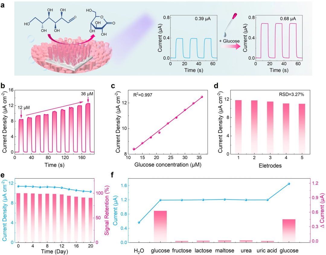 Figure 5. Demonstration of PEC glucose sensing using p-n GaN/CoNiOₓ photoelectrodes. (a) Schematic diagram of the PEC glucose sensing mechanism of p-n GaN/CoNiOₓ photoelectrodes; (b) Relationship between photocurrent and time of p-n GaN/CoNiOₓ photoelectrodes with continuous addition of glucose under 340 nm chopped illumination; (c) Linear relationship between photocurrent and glucose concentration; (d) Repeatability experiment of five sets of parallel-prepared p-n GaN/CoNiOₓ photoelectrodes under 30 μM glucose conditions; (e) Stability test of p-n GaN/CoNiOₓ photoelectrodes under 30 µM glucose conditions. The photoelectrodes were stored under dry and room temperature conditions; (f) Detection of interference of substances such as fructose, lactose, maltose, urea, and uric acid on photocurrent in the electrolyte.
Author Information
 Zongzhi Yin
Corresponding Author
Chief Physician, First Affiliated Hospital of Anhui Medical University▍Main Research Areas Mainly engaged in the study of uterine contraction mechanisms during pregnancy, focusing on the abnormal regulation of pregnancy maintenance and perinatal period due to nutritional metabolic disorders (including obesity and diabetes).
▍Personal Profile
Chief Physician of Obstetrics and Gynecology at the First Affiliated Hospital of Anhui Medical University, Deputy Director of Obstetrics and Gynecology Education and Teaching, Deputy Director of the Key Laboratory of Reproductive Disorders and Obstetric Diseases in Anhui Province. Selected as an A-class innovative talent in the ninth batch of the “Special Support Plan” in Anhui Province, a reserve candidate for leading academic and technical talents in Anhui Province, and one of the first outstanding talents recognized by the Anhui Provincial Health Commission. He has presided over three National Natural Science Foundation projects and has led/participated in more than ten national and provincial-level projects, receiving a second prize for scientific and technological progress in Anhui Province. Currently serves as a member of the Reproductive Science Committee of the Chinese Physiological Society, a youth committee member of the Perinatal Medicine Branch of the Chinese Medical Association, a youth committee member of the Obstetrics Group of the Obstetrics and Gynecology Branch, a member of the Obstetrics and Gynecology Branch of the Anhui Medical Association, and a standing committee member of the Maternal-Fetal Medicine Branch of the Provincial Physician Association.
▍Email:[email protected]
 Haiding Sun
Corresponding Author
Professor, University of Science and Technology of China▍Main Research Areas Research on the epitaxy of third-generation semiconductor gallium nitride (GaN) materials (including nanowires, thin films, etc.) and their applications in optoelectronic and electronic devices.
▍Personal Profile
Professor/PhD supervisor at the School of Microelectronics, University of Science and Technology of China, and head of the iGaN Lab. Selected as a National Excellent Young Scholar, Anhui Province Outstanding Young Scholar, and a high-level talent from the Chinese Academy of Sciences. He has long been engaged in research on the epitaxy of gallium nitride (GaN) semiconductor materials and device design and fabrication. His research results have been featured on the covers of authoritative semiconductor journals such as “Compound Semiconductor” and “Semiconductor Today” multiple times. Currently serves as an associate editor for several international journals such as IEEE Photonics Technology Letters and Journal of Semiconductor, and is a committee member for various international optoelectronic conferences such as CLEO/IEEE IPC. He has also been awarded the iCAX Young Scientist Award and the 2021 IAAM Young Scientist Medal. He leads national key research and development projects, National Natural Science Foundation projects, and provincial-level projects. He has published over 150 SCI papers, including in Nature Electronics and Advanced Materials.
▍Email:[email protected]
Written by: Original authors Edited by: Editorial Department of Nano-Micro Letters (English)
About Us
 Nano-Micro Letters is an academic journal sponsored by Shanghai Jiao Tong University and published open-access by Springer Nature, primarily reporting high-level articles related to nano/micro-scale research (research articles, reviews, communications, perspectives, highlights, etc.), including the synthesis, characterization, and performance of micro-nano materials and structures, as well as their applications in energy, catalysis, environment, sensing, electromagnetic wave absorption and shielding, and biomedicine. It has been indexed by SCI, EI, PubMed, SCOPUS, and other databases, with a 2022 JCR impact factor of 26.6, ranking in the top 5% of Q1 in its field, and is a top journal in the first district of the Chinese Academy of Sciences. It has received multiple honors such as “China’s Most Internationally Influential Academic Journal,” “Outstanding Science and Technology Journal of Chinese Universities,” and “Shanghai’s Excellent Science and Technology Journal,” and was nominated for the “China Publishing Government Award Journal Award” in 2021. We welcome your attention and submissions.Web: https://springer.com/40820E-mail: [email protected]
Tel: 021-34207624






Scan the QR code above to follow us
Click to read the original text/ Scan the mini-program code above to get the English original for free